Common SMT Soldering Defects and How to Avoid Them in PCB Assembly
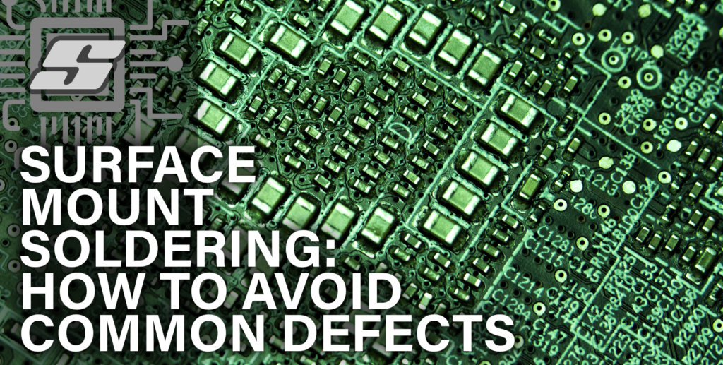
Surface mount technology (SMT) soldering is a widely used technique in producing printed circuit boards (PCBs).
SMT soldering allows for the placement of electronic components onto the surface of a PCB rather than inserting them through holes in the panel. This technique provides many benefits, such as improved component density and reduced manufacturing time.
However, SMT soldering can also result in defects that can affect the reliability and functionality of the final product. Below are some of the most common SMT soldering defects and how to avoid them in PCB assembly.
Solder Bridging
Solder bridging occurs when excess solder connects two adjacent pins or pads on a PCB, creating an unintended electrical connection. Solder bridging can happen for several reasons, including excessive solder paste application, misalignment of components, or incorrect temperature profiles during reflow soldering.
Proper stencil design and solder paste application are crucial to avoid solder bridging. The amount of solder paste applied should be appropriate for the size of the pad or pin, and the paste should be evenly distributed. Using a solder mask or dam can also prevent excess solder from spreading and causing bridging. In addition, careful placement and alignment of components and proper temperature profiles during reflow soldering can help prevent solder bridging.
Tombstoning
Tombstoning occurs when a component lifts and stands on one end during reflow soldering, creating an open circuit. Tombstoning can occur for several reasons, including uneven heating during reflow soldering, improper pad design, or incorrect component placement.
To avoid tombstoning, proper component placement and alignment are essential. The pads on the PCB should be designed to provide equal and adequate heating during reflow soldering. In addition, using a solder mask or dam can help prevent components from lifting during reflow soldering.
Insufficient Solder
This incident occurs when there is not enough solder applied to a pad or pin during soldering, resulting in poor or non-existent electrical contact. Lack of solder can ensue for several reasons, including incorrect solder paste application, improper temperature profiles during reflow soldering, or inadequate flux activity.
Proper solder paste application and temperature profiles during reflow soldering are crucial to avoid insufficient solder. The solder paste should be evenly applied to the pad or pin, and the temperature profiles should be exact for the size of the component and the PCB. In addition, using high-quality flux can help ensure adequate wetting and adhesion of the solder.
Lifted Pads
Lifted pads occur when a pad on a PCB lifts from the board, creating an open circuit. These can occur due to several reasons, including improper pad design, excessive mechanical stress during assembly, or inadequate pad adhesion to the board.
Avoid lifted pads with proper pad design and utilization of assembly techniques. The pads on the PCB should be designed to provide adequate adhesion and mechanical strength. In addition, using ESD-safe tools and avoiding excessive mechanical stress can help prevent lifted pads.
Voiding
Voiding is the formation of small air pockets within the solder joint. It can manifest due to various reasons, including inadequate flux activity, improper temperature profiles during reflow soldering, or low-quality solder paste.
Proper solder paste application and temperature profiles during reflow soldering can help minimize voiding. Apply the solder paste evenly and only use the appropriate amount. The temperature profiles should be suitable for the size of the component and the PCB, and the use of high-quality flux can help ensure adequate wetting and adhesion of the solder. In addition, using a vacuum-assisted reflow process can help reduce the formation of voids in the solder joints.
Solder Balling
Solder balling occurs when small, spherical balls of solder form on the surface of the PCB, often near the edges of components. Solder balling can occur for several reasons, including excessive solder paste application, incorrect temperature profiles during reflow soldering, or contamination of the PCB surface.
Proper solder paste application and temperature profiles during reflow soldering are crucial to avoid solder balling. The amount of solder paste applied should be appropriate for the size of the pad or pin, and the paste should be evenly distributed. The temperature profiles should be appropriate for the size of the component and the PCB. In addition, proper cleaning and preparation of the PCB surface can help prevent contamination that can lead to solder balling.
Hiring PCB Companies for SMT Soldering
SMT soldering is a critical process in PCB assembly, but it can also lead to several common defects that can affect the reliability and functionality of the final product. Proper design, handling, and assembly techniques are essential to avoid these defects. Utilizing high-quality materials, such as those provided by ELE PCB, can also help ensure the success of your PCB assembly project.
ELE PCB is a reputable company that provides high-quality PCB materials and assembly services. As such, hiring SMT soldering services from PCB manufacturers like ELE PCB solves many problems at once, keeping the cost minimal while your corporation focuses on other things.
ELE PCB’s products and services are designed to satisfy the demands of a broad range of customers, from hobbyists to large corporations. They use advanced manufacturing processes to ensure they deliver the highest quality and meet the industry’s most stringent standards.
In summary, to avoid common SMT soldering defects in PCB assembly, it is essential to follow proper design, handling, and assembly techniques. Additionally, utilizing high-quality materials and professional services would help ensure that these rejects and possible accidents may be avoided, while you pursue a successful PCB assembly project on various scales.
Thanks so much for visiting my site! If this article helped you achieve your goal and you want to say thanks, you can now support my work by buying me a coffee. I promise I won't spend it on beer instead... 😏