Wanting to make a PCB but don’t know where to start? The goal of this super quick and easy tutorial is to get you started in PCB design!
Perhaps you have only just embarked on the journey of learning how to turn new and imaginative ideas into working electronics projects.
Perhaps you already know about EAGLE design software and that the maker community and most hobbyists tend to choose it for PCB design.
Perhaps you even have your first schematic complete and are stuck with taking the next step, turning it into a board.
In the previous two tutorials in this series we covered the process of making a schematic and the process of making a custom library component.
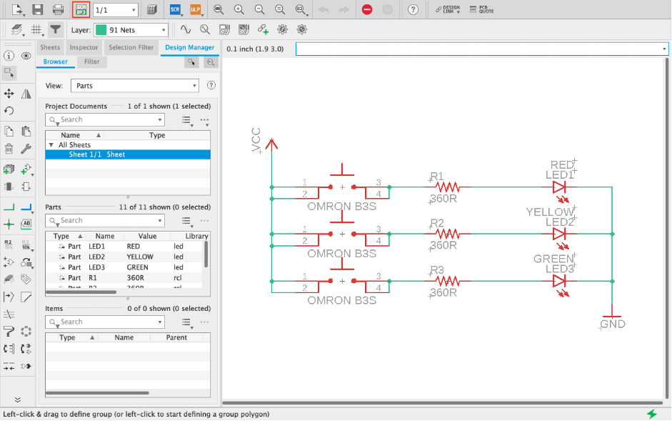
In order to create a new board we first need a finished schematic. If you arrived here with your own completed schematic ready to go, great!
If you don’t yet have a completed schematic then I would recommend that you work your way through the first tutorials in this series.
- How To Turn An EAGLE Schematic Into A Board
- How To Place Components On The Board
- How To Use The EAGLE Ratsnest
- How To Manually Route Traces In EAGLE
- How To Use The EAGLE Autorouter
- How To Create A Ground Plane In An EAGLE Board Design
- Whats Next…?
How To Turn An EAGLE Schematic Into A Board
For the purpose of this tutorial we will be using the previously created schematic, but you can use your own.
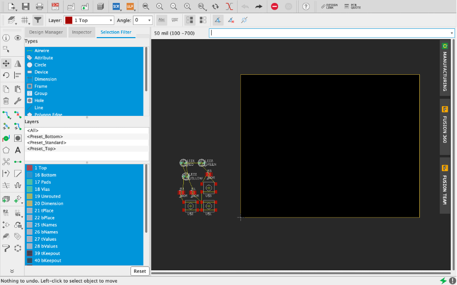
First of all, go ahead and open your schematic. Then click the BRD tool on the left-hand side of the upper toolbar, to create a new board.
This will open a new board editing window with the components ready to be placed.
In EAGLE the schematic and board editors are almost like two separate programs, however the two must remain congruent. It is important to keep both files open at the same time in order to prevent problems.
How To Place Components On The Board
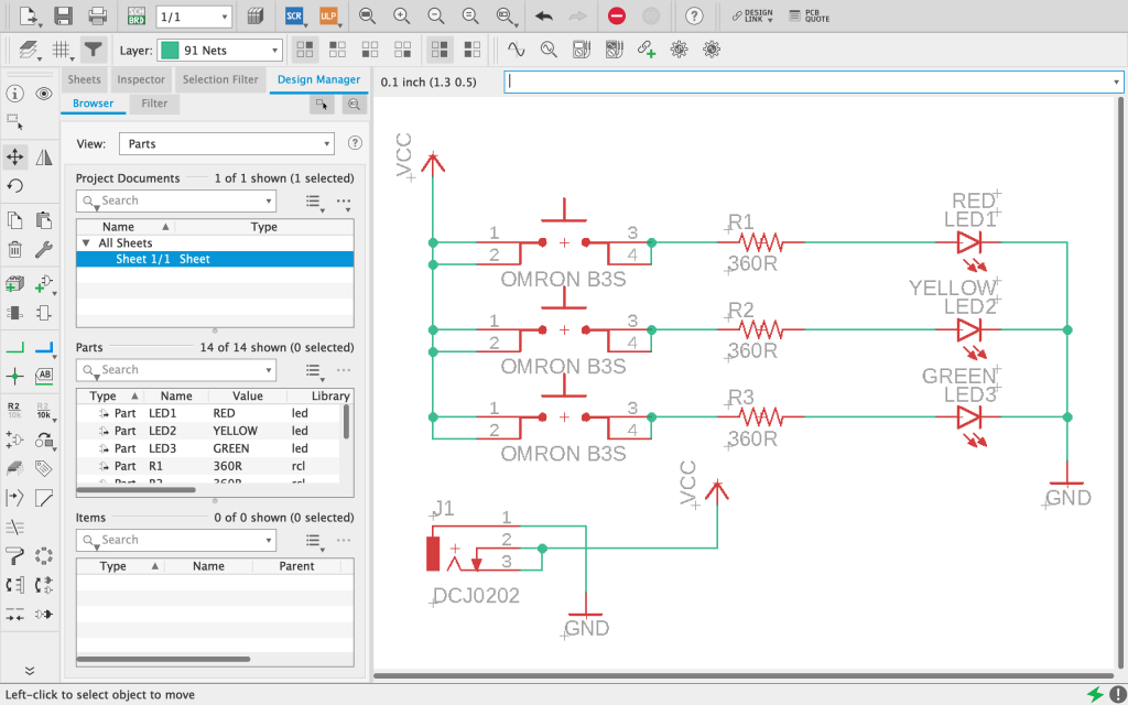
When a new board is created, you will be presented with a pile of components and an empty board space.
The components placed in the schematic will be laid out and must be placed within the board area.
At this stage you can use the move tool to change the board size, but usually I prefer to first place the components into a space greater than necessary in order to have some free room to move them around during figuring out the layout.
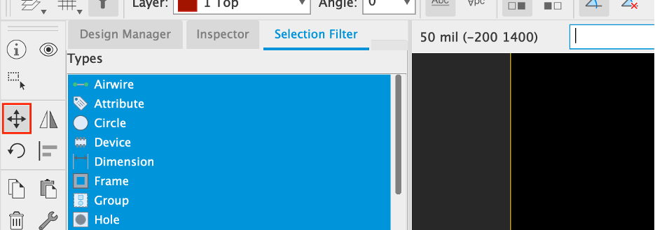
First we will use the move tool in order to place the components in the desired location.
Choose the move tool from the left-hand toolbar and then click the origin (+) of the component in order to pick it up.
Move it to the desired position and click to place it. If you are using the sample schematic from the previous tutorial, you can place the components as shown in the following screenshot.
How To Use The EAGLE Ratsnest
You may already have an idea where you would like to place components on the board, however we must consider how the traces will be routed in order to make all of the electrical connections specified in the schematic.
Each connection is shown in what is called the ratsnest. Each pad that requires a connection has a yellow line between it and the point it needs to connect to.
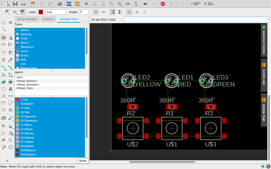
When a trace is drawn between the pad and its point of connection, the yellow line will disappear. The goal is to place components, then route traces until the ratsnest has gone and routing is 100% complete.
Sometimes when a lot of components are placed, the ratsnest can become very complex and messy.
You can simplify it at any stage by pressing the ratsnest button on the left-hand toolbar.
You may also want to hide the ratsnest at some stages during the design, as at times it can get in the way.
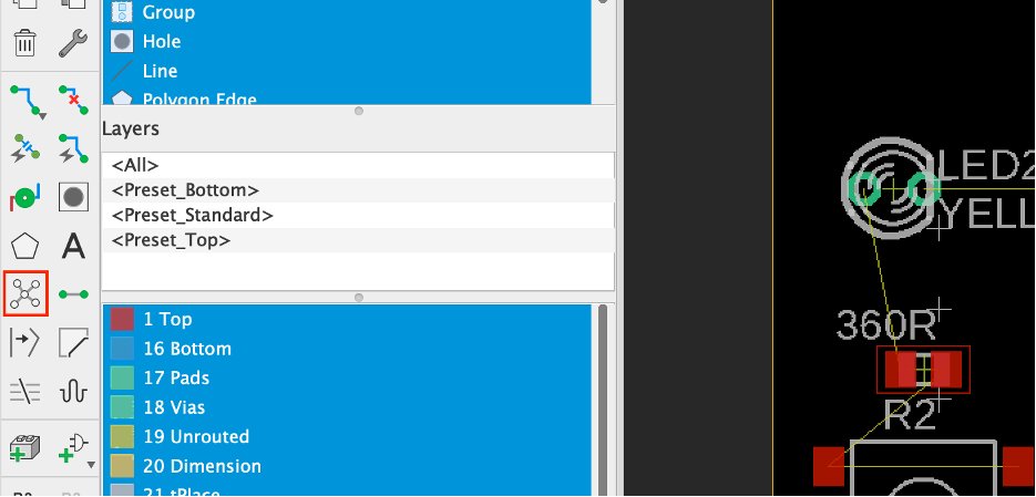
There are different layers within a board design in EAGLE, each containing different data related to the board design.
The ratsnest is also allocated to its own layer and therefore can be hidden.
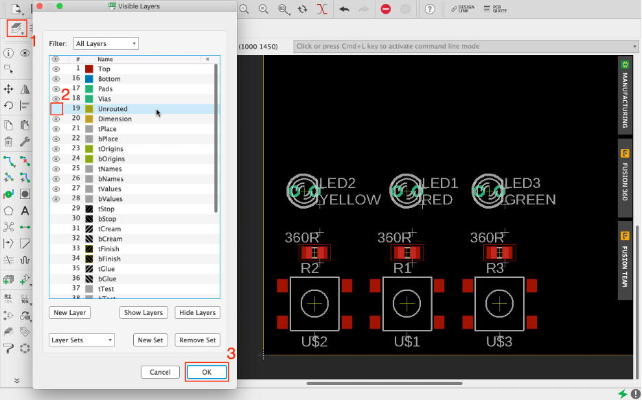
First click on the layer button at the far left of the top toolbar. This will open the visible layers window.
In order to show or hide a layer, click the small eye icon next to the layer. If the eye is not present, the layer will be hidden. Hiding the unrouted layer will hide the ratsnest.
How To Manually Route Traces In EAGLE
Now that we have an understanding of the ratsnest and how to use it, we can begin routing traces.
First, we will learn how to manually route traces. Although EAGLE comes with a fairly competent auto router, I always find better results are achieved when routing by hand. The auto router does have its uses though, more on that later.
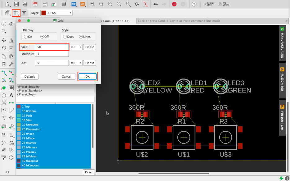
Before we start routing, we should choose our preferred units. This will be down to personal preference.
To change the units, click the grid tool on the left-hand side of the top toolbar. For this tutorial I will leave the default grid spacing as 50 mil.
If you prefer metric then you can change it with the units drop down box. Once you are happy with the settings, click ok.
Now that we have the grid and units set as desired, we can begin routing traces.
First choose the route airwires tool from the left-hand toolbar. With the tool selected it’s possible to alter the parameters of the trace on the toolbar along the top of the screen.
In this example I have changed the default 6 mil trace to a 20 mil trace.
Note that you can also specify the units when entering values into EAGLE parameters. Regardless of the grid settings, we could still enter 0.5mm here and EAGLE would convert it to the native units.
Once the trace width has been set, click the pad you wish to connect. The net will become highlighted, showing the areas where we could connect the trace.
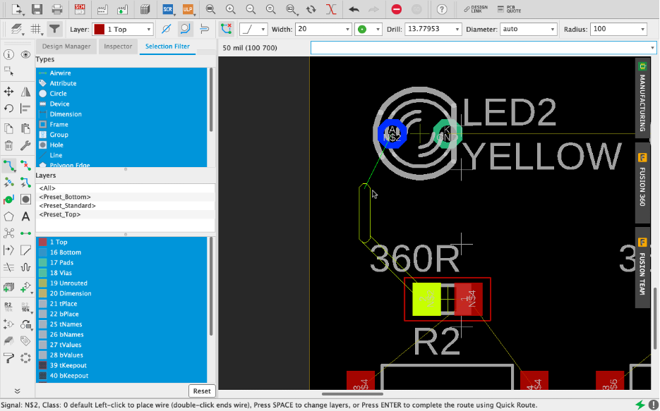
Whilst the trace is being generated and it is following the mouse pointer, you can click to place and then continue to route, giving you control over where the trace is routed.
We ultimately need to route the trace to one of the highlighted pads in order to make the connection. Once a connection is successful, the corresponding ratsnest airwire will disappear and a trace will be placed.
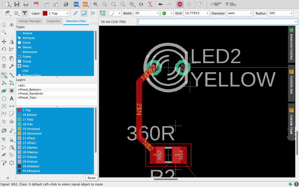
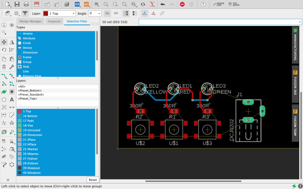
Congratulations! You have laid down your first PCB trace! Now we can repeat this with each of the other three LEDs.
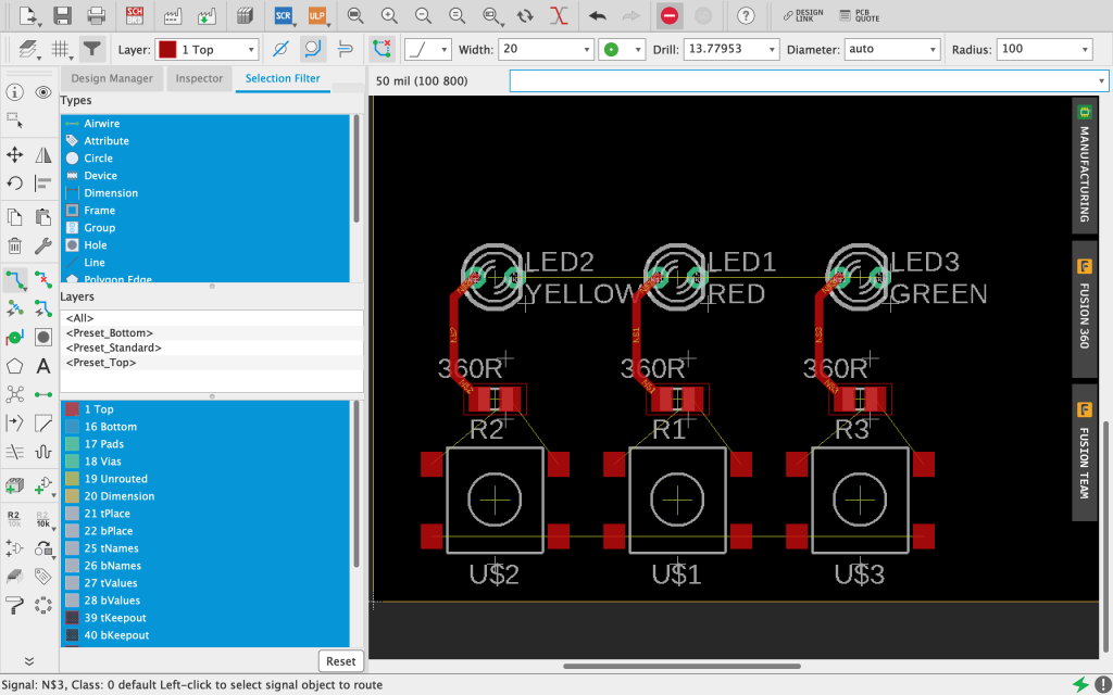
So now we have successfully routed the first three traces, which are showing in red to indicate that they are placed on the top layer.
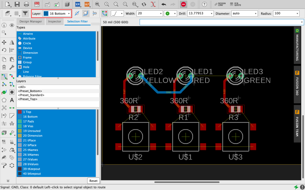
However it is also possible to route traces on the bottom side of the PCB. This is a very necessary part of PCB design and it allows us to cross over the existing traces on a different layer.
It is possible to have many more layers within a PCB design and the Pro version of EAGLE supports up to 16 different layers.
However the free version here allows only the top and bottom layer to be used. This is usually enough for most basic designs and is less of a limitation for the hobbiest.
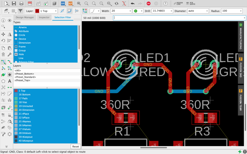
In order to draw a trace on the bottom layer, simply select the bottom layer from the layer drop down and then draw the trace in the same way as before.
Notice how it is possible to cross over traces on the bottom layer without generating an error.
This is possible because the blue traces will be manufacturing on the bottom side of the board and connections will be made between the layers using plated through holes.
In this first example we have taken advantage of a plated through hole in the board, which will be drilled in order to mount the LED.
As this hole passes through the entire board, it is possible to connect it on both the top and bottoms sides.
But what about the surface mount components? In this example they are all placed on the top side surface of the board, with no plated through holes.
It is also possible to transition a trace from the top to the bottom side and vice versa at any point on the board using a via hole.
A via is a plated through hole that is usually smaller than a component plated through hole, which serves only as a transitional point between layers.
In PCB manufacturing, drill diameters are usually specified in metric units. EAGLE defaults to a 13.77 mil via, which equates to a 0.35mm hole diameter.
It seems very small but this is actually a very common size and easy to drill! Via holes can be mechanically drilled down to around 0.1mm diameter and even smaller when laser drilling is used.
However it would be advised to keep the size above 0.3mm diameter where possible in order to keep costs lower, as there is no need to make a board more difficult to manufacture than what is necessary.
Note that it is possible to enter both metric and imperial units into EAGLE, regardless of what is set as the operational units. Let’s set the via size to 0.4mm by entering it into the box on the top toolbar.
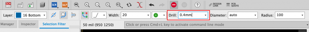
Note that when you press enter, the value will change to the operational unit, in this case an imperial value of 15.74 mil.
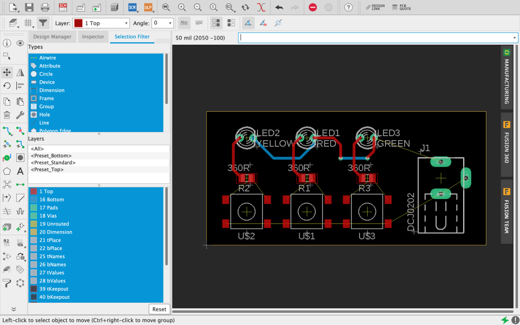
Next set the layer to the top layer and begin to draw a trace from the unconnected pin on LED 3. Left-click just below the LED in order to anchor the trace to that location on the board and then change the layer to bottom.
Note that the trace will follow the cursor as you go to change the layer to bottom, you can ignore this as it is just a quirk of EAGLE.
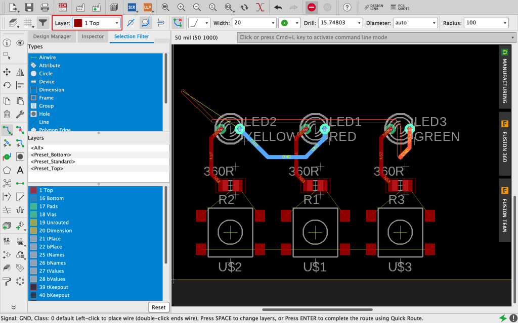
Once you have changed the layer to bottom, you will be able to place a via hole. The point in which you place the hole will be the point the trace transitions to the bottom layer.
In this example we can place the via at the end of the top-side trace just drawn and then cross the neighbouring top-side trace using the bottom layer.
Once on the other side of the neighbouring trace, we can transition back to the top of the board and continue to route the trace.
The more vigilant amongst you may have noticed that it was not necessary to jump back to the top layer in order to connect the LED and only one via was required!
How you route the traces and optimise the design is entirely your own decision… and in my opinion it adds the creativity and excitement to the process! This is merely an example to demonstrate the tools.
How To Update The Board From The Edited EAGLE Schematic
From time to time it will be necessary to make changes to the design during the process of placing components and routing traces.
Perhaps you noticed an error that needs correcting, or need to add something to the design.
In this example it may already be evident that we did not add a power supply to the design. Therefore we can return to the schematic editor in order to add one.
Clicking the sch/brd button on the top toolbar will result in the schematic being opened.
It is important to keep both open during board design, in order for the board and schematic to remain congruent. Not doing so will result in the error no forward/back annotation will be performed.
Let’s add a DCJ0202 power jack to the design. Locate the component in the component editor and add it to the schematic. If necessary you can refer back to the earlier tutorial on schematic design in EAGLE in order to learn how to do so.
Note that nets do not have to be physically connected by green lines in order to be connected. Simply giving the nets the same name will result in them being connected within the board design.
In this case creating a second Vcc and GND within the design will connect the nets to the existing nets with the same name.
Click the sch/brd button again to return to the board editor. You will now see the new component footprint and associated ratsnest. You can place the component in the desired location.
How To Use The EAGLE Autorouter
So far we have routed some of the traces, connecting the LEDs to their associated resistors. In order to route the remaining traces, we will use the autorouter.
The autoroute tool will calculate routes for the remaining traces and lay them down on the board automatically. It has the ability to give several different solutions and different levels of optimization.
The autorouter will work within the confines of the board profile, therefore at this stage we need to use the move tool to resize the board profile.
Simply select the move tool and click either the middle or the corners of the board profile to change the shape and size.
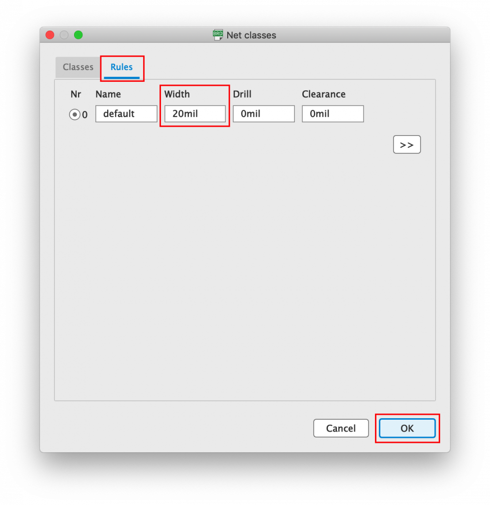
Next we need to configure something called net classes. This will allow us to specify to the autorouter the widths for different groups of nets.
As this is our first basic design we will simply configure the default net class and set the overall trace width to 20 mil.
Click on Edit > Net Classes to open the dialog box. Then click on the rules tab and set the width to 20 mil and then click ok.
Once the net class is configured, we can open the autorouter by clicking the autorouter tool from the side toolbar.
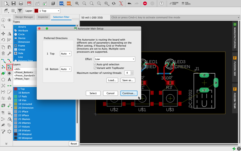
We won’t dive too deeply into the configuration and in most cases for simple designs the autorouter default settings will work just fine. On the first screen we will leave everything as it is and click continue.
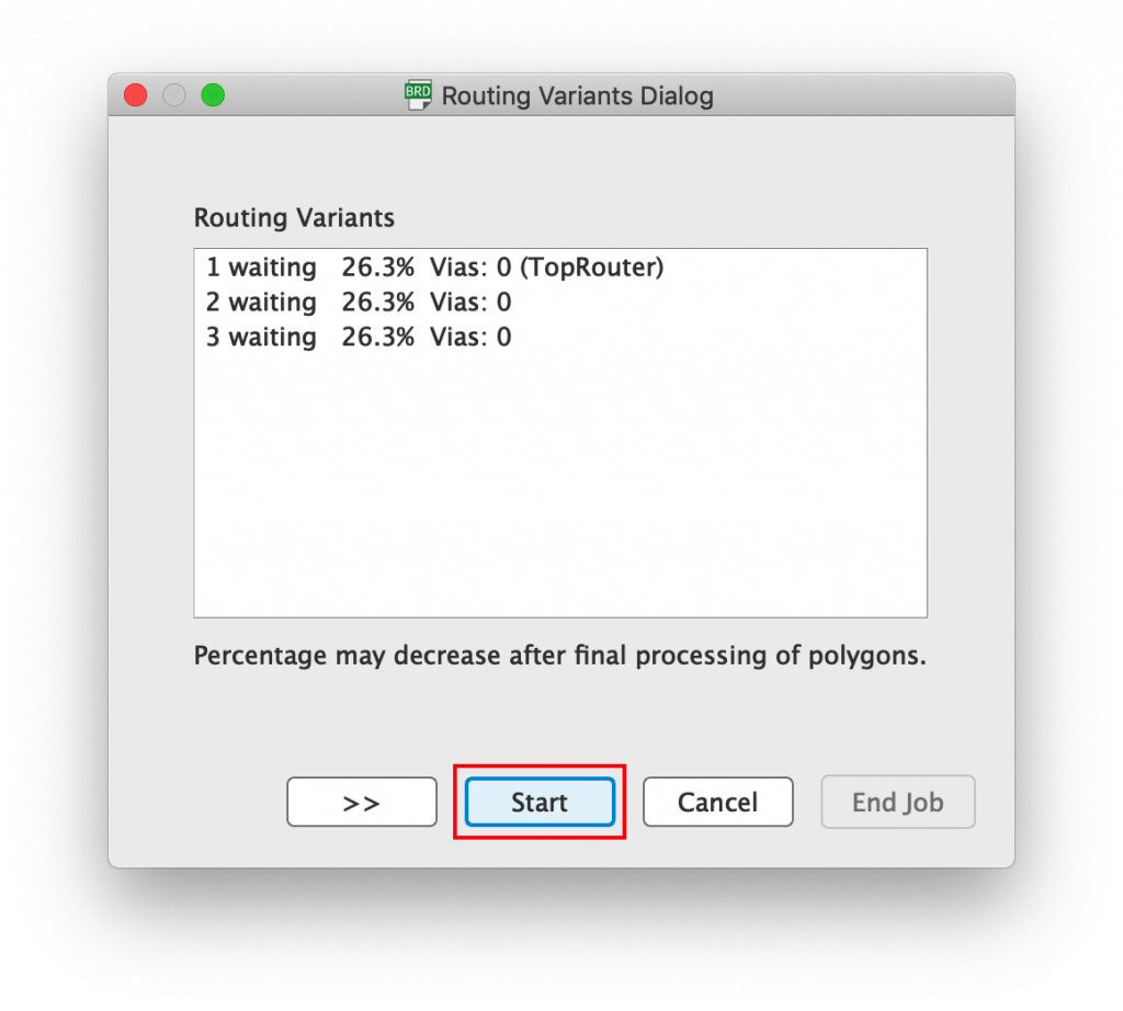
This will open the routing variants dialog box. Simply click start to begin autorouting.
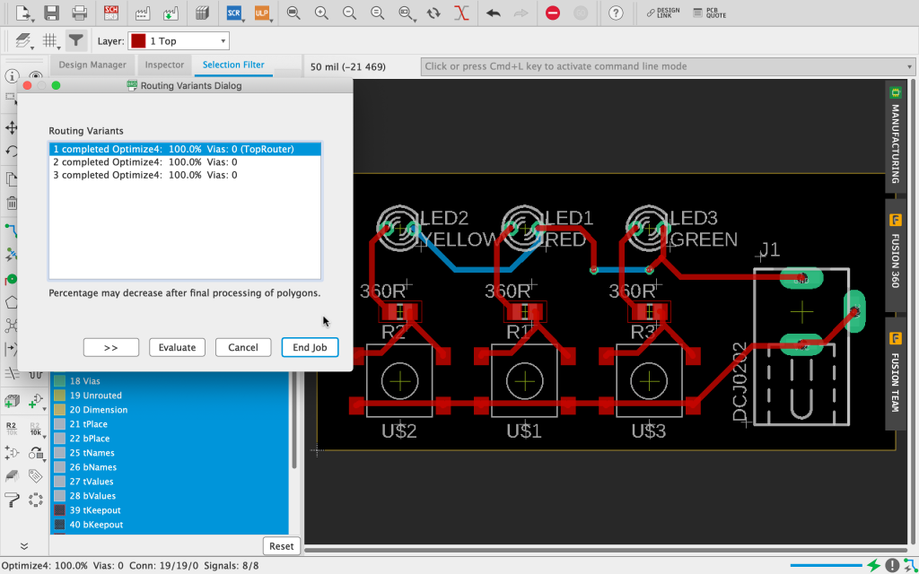
Once the autorouter has finished, you can choose between several options for routes. Click on the different routing variants in order to view the different solutions.
In the following screenshot we can see the first route optimization.
By comparison we can see that the second route optimization has some differences, most notably around the push switches.
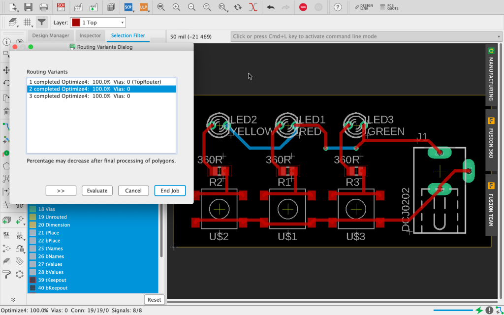
For a simple design it may be more difficult to see the benefit of having different optimizations. However as your designs progress, you will find that the different optimizations become more relevant and useful.
Congratulations! You have successfully completed the autorouting and now the board is 100% connected.
In the bottom left-hand corner of the screen you should now see the message stating that the routing is 100% complete.
How To Create A Ground Plane In An EAGLE Board Design
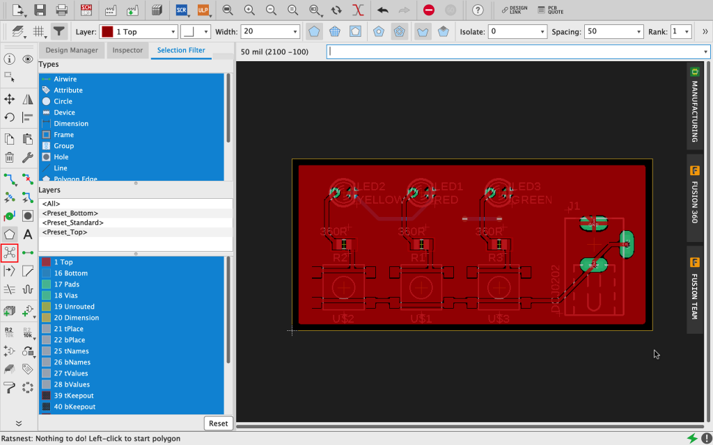
The last thing we need to do in order to complete the board is to flood the unused areas with copper. This copper flood is usually referred to as a plane and it is generally a good rule of thumb to connect this to the GND net.
In order to create a plane, select the polygon tool from the left-hand toolbar. Click in one corner of the board on top of the profile to begin drawing a line.
Click the adjacent corner to draw the first line, repeat for each remaining corner until you arrive at the first corner.
Once you click the corner where you began, a square polygon will be placed. EAGLE will ask you for a name for the net. Name the net GND in order to connect the plane to the GND net.

In order to make it easier to edit a complex board, EAGLE does not draw the plane by default. In order to draw the plane, simply click the ratsnest button from the left-hand menu.
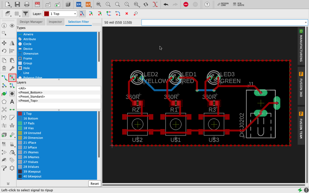
If you wish to remove the flood in order to better see the detail in the board, you can use the ripup tool. Select the ripup tool and click the edge of the polygon.
What’s Next…?
A big well done to you! You have successfully completed the tutorial and hopefully now you have a grasp on the basic tools required in order to create a board layout in EAGLE.
There are many other more advanced tools that become more relevant as your board designs grow in complexity. We will cover these in later tutorials.
So maybe you are wondering how you can turn your wonderful new board layout into a real life circuit board?!
In the next tutorial we will cover the CAM processor and steps required in order to output all of the data required to order a PCB from a board fabricator.
The next installment of the EAGLE tutorial series coming very soon…
Thanks so much for visiting my site! If this article helped you achieve your goal and you want to say thanks, you can now support my work by buying me a coffee. I promise I won't spend it on beer instead... 😏