
Making a custom library component in EAGLE can at first seem a little daunting! The library editor is not dissimilar in complexity to the schematic or board editor.
Well prepare to be surprised as this tutorial shows you just how easy it can be as we walk through the process step by step.
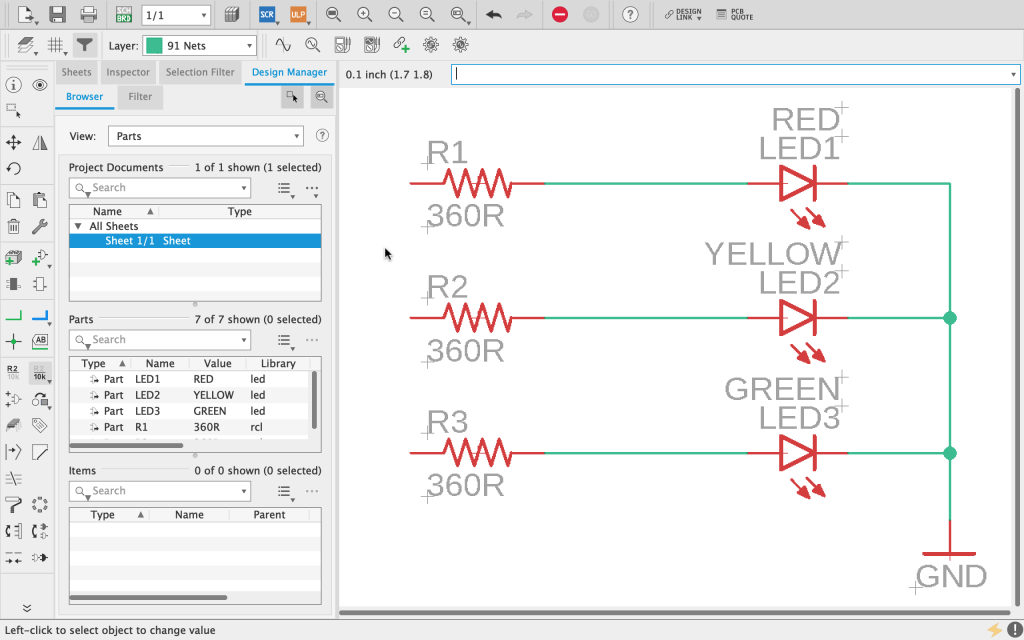
In the first article in this series we learned how to make a schematic in EAGLE using standard library components.
If you are new to EAGLE or PCB design in general then it is definitely worth checking out, however not necessary if you just wish to learn how to make custom library components.
Contents
- Create a Library
- Create a Footprint
- Create a Symbol
- Create a Device
- Placing a Custom Device Into a Schematic
- What’s Next…?
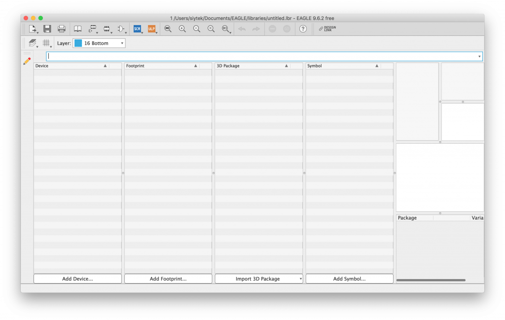
Create a Library
EAGLE has a library editor that allows us to create new libraries with custom components. In order to open it, from the welcome screen, click File > New > Library.
Each component in the library consists of four parts, the device, footprint, 3D package and symbol. It is not necessary to include a 3D model, so we will focus on the three necessary parts.
The symbol is featured in the schematic design and can be tied to one or more different footprints that will appear within the PCB board design.
If the particular component you are creating is available in multiple packages, it is possible to include the different package variants.
The symbol and various packages are combined by creating the device. This allows us to choose which pins in the symbol are connected to which pins on the footprints.
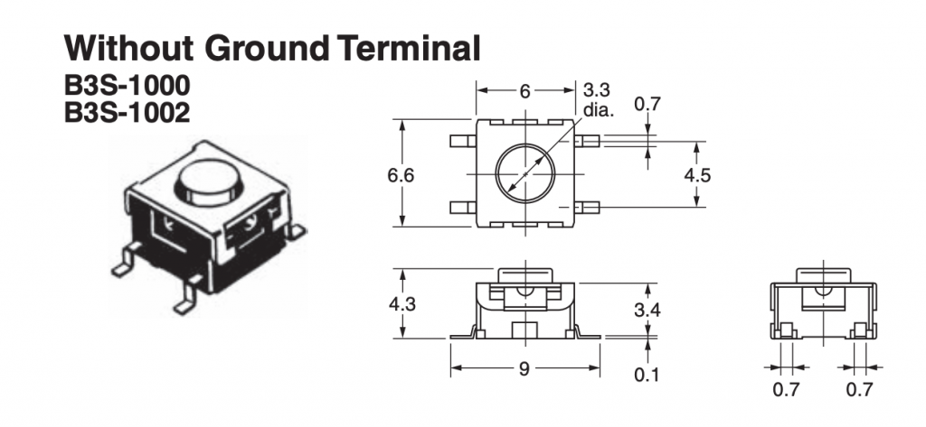
For this example we will create a library component for the Omron B3S switch, you can download the datasheet here. If you are new to datasheets, check out this tutorial detailing how to interpret them over at Sparkfun.
Create a Footprint
First we will create a footprint for the device. This is the actual design that will appear on the PCB, consisting of the copper pads, soldermask openings and silkscreen component markings (usually white ink on the PCB).
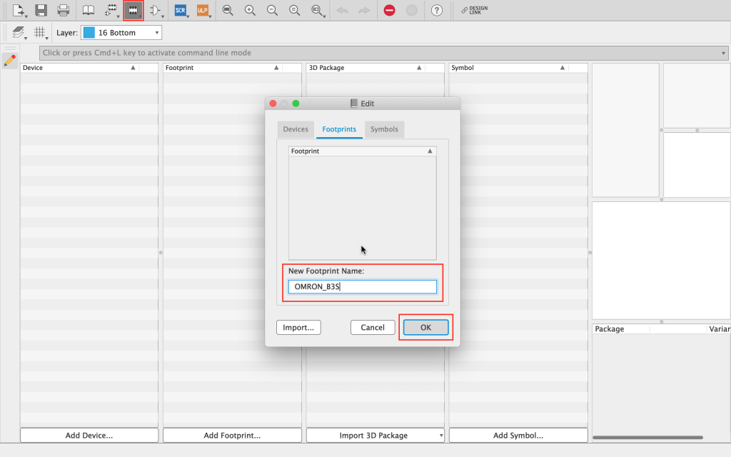
First click on the new footprint button at the top of the screen.
A dialog box will open, enter a name for the new footprint and click ok. EAGLE will ask you to confirm if you want to make a new footprint with your chosen name, click yes.
Next we can take a look on page 2 of the datasheet. Here we will find the dimensions given for the land required for the button.
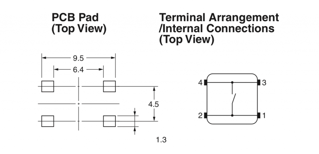
In order to create this footprint, we will create the 4 pads shown in the datasheet as surface-mount pads. First we must consider that in EAGLE, these pads will be placed using a central co-ordinate.
From the datasheet we need to calculate the size of the square pads and the coordinates for the center points.
The height of the pad is given as 1.3mm.
We can calculate the width by subtracting 6.4 from 9.5 and then dividing by 2, to get 1.55mm.
We now know that the pad dimensions are 1.3 x 1.55mm.
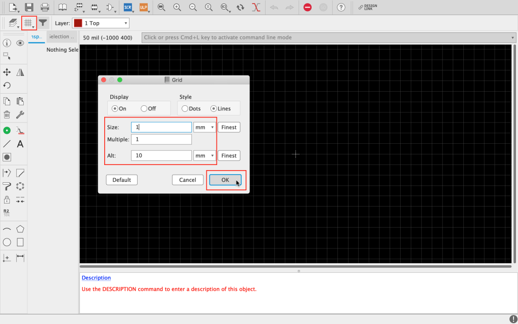
As we are working in metric, first we can change the default dimensions from imperial to metric. In the top left of the screen, click the grid button and change the size to 1mm.
You can also set an alt value too, in this case 10mm. This is the value that the snapping will temporarily change to whilst you hold down the alt key.
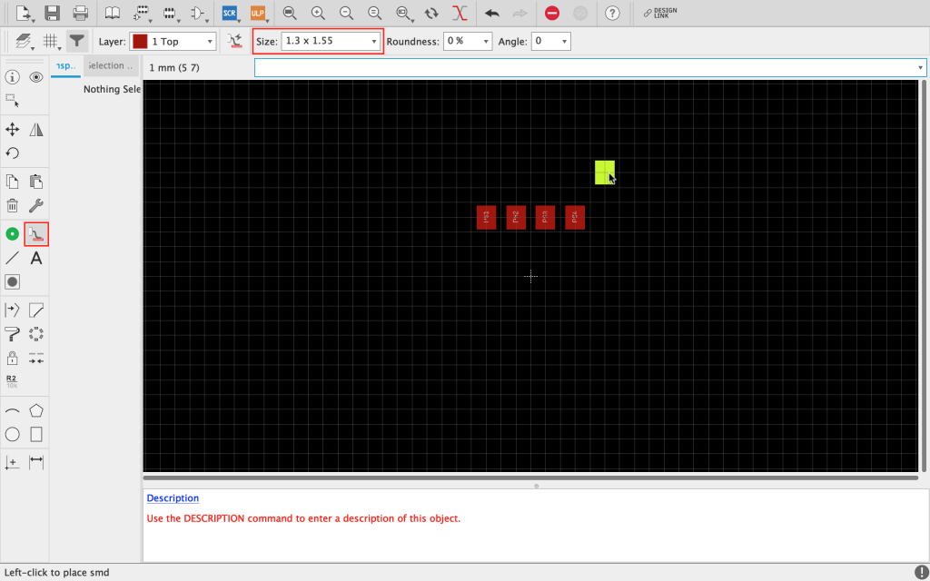
Now click on the SMD tool on the left-hand side of the screen and enter the pad size in the box at the top as shown in the screenshot below.
Then place 4 SMD pads somewhere just above the 0,0 origin (the small + in the middle of the workspace). At this state the exact location is not important as we will manually enter the coordinates to locate them exactly.
In order to position the pads correctly, we need to calculate the central positions of each pad shown in the diagram in the datasheet.
The Y axis dimension is given as 4.5mm and as the origin point is shown in the middle, we can divide this by 2 giving 2.25 and -2.25 for the Y axis positions of the top and bottom pads respectively.
For the center point on the X axis we need to take the 6.4mm dimension that is given, divide it in half and then add half of the known pad width, in order to get the center point.
This gives us an X axis position of -3.975 and 3.975 for the left-hand and right-hand pads respectively.
Now we have all of the coordinates required to place the pads.

In order to move the pads the calculated coordinates, first right-click the origin of the pad ( the + in the center) and select properties.
A dialog box will open, you can manually change the position attribute to match the values in the diagram above, as shown in the following screenshot.
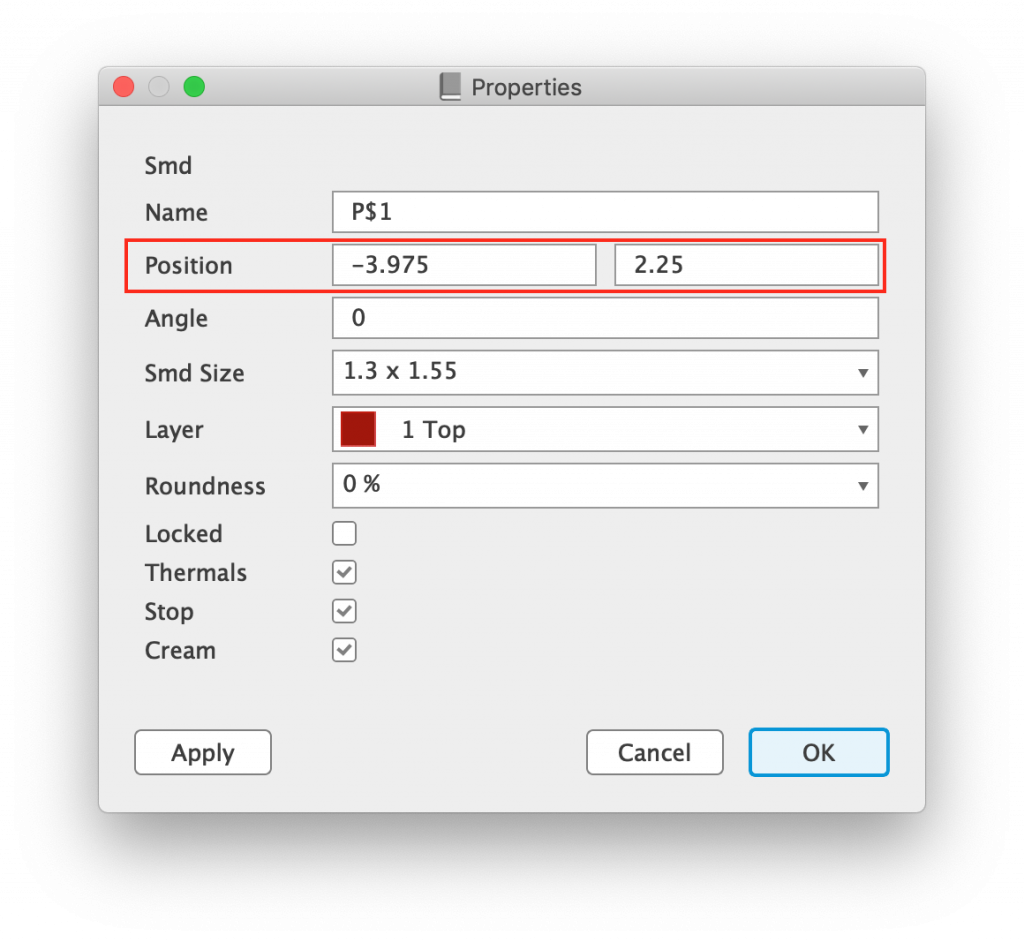
Once the position attribute has been changed, click ok and then repeat this for each of the remaining pads.
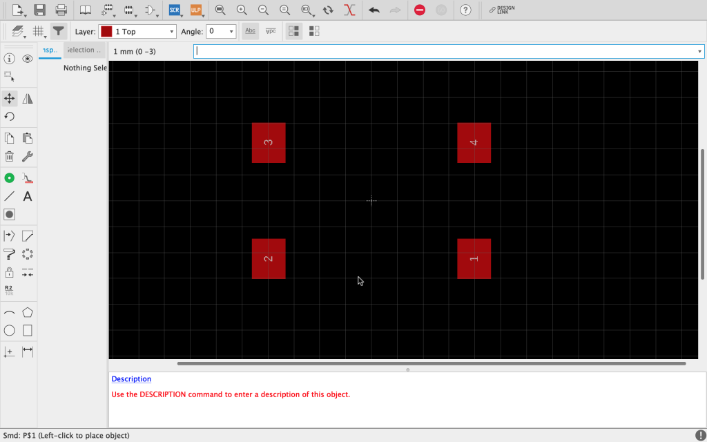
You can also change the name of each pad to match the diagram in the datasheet. This can either be done in the properties dialog shown above, or directly by right-clicking the pad origin and choosing name.
Once the positions and name attributes have been edited, you should end up with a footprint that looks just like the diagram in the datasheet.
Now the copper data is complete and the soldermask layer will also have been created automatically, as SMD pads were used.
To complete the footprint we will add some silkscreen marking that identifies the component. This will be printed (usually) in white ink by the PCB manufacturer.
Looking in the datasheet we can find the mechanical dimensions of the switch. You will notice the outer diameter of the casing is 6mm x 6.6mm and there is a 3.3mm diameter button in the center.
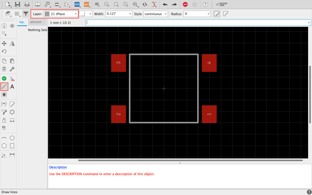
First we will draw a box to represent the switch casing outline.
Select the line tool on the left-hand side and change the layer to tPlace at the top of the screen. This will place the lines on the top silkscreen layer rather than the default top copper layer.
Using the grid, draw a 6mm by 6mm box with the main (+) origin in the center, as shown in the following screenshot.
Next we can right-click the top line (somewhere near the middle) and choose properties. Here we can see there are coordinates that define where the line begins and ends.
We can edit the Y axis coordinate and change it from 3 to 3.3 as shown in the following screenshot.
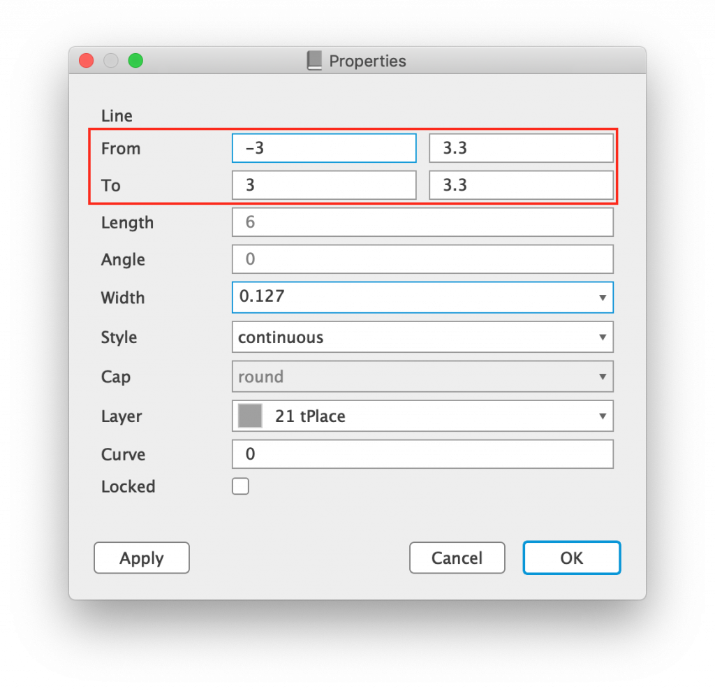
Once the value is changed, click ok and repeat for the bottom line. This will extend our box along the Y axis to 6.6mm to match the drawing, as shown in the following screenshot.
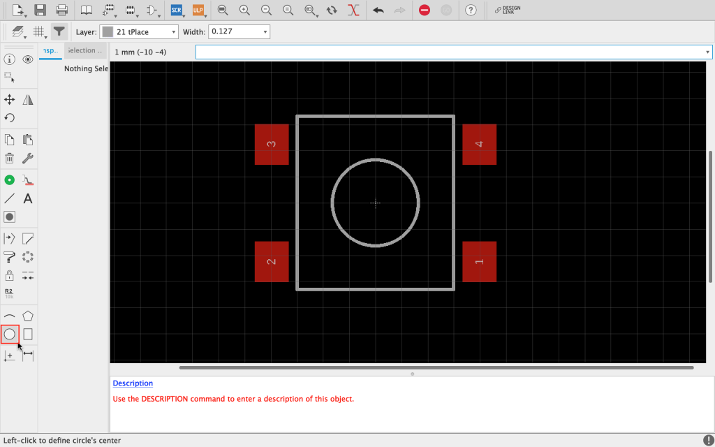
Lastly we can use the circle tool to add the 3.3mm diameter circle in the middle. Simply draw a circle from the main origin that is roughly the correct size.
Once the circle has been placed, right-click it and change the radius attribute to 1.65 in order to get a finished diameter of 3.3mm as shown in the screenshot below.
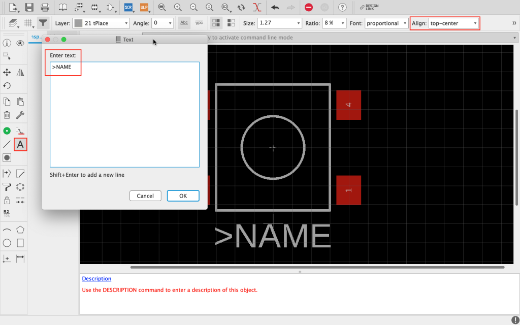
Lastly we can add some labelling to our component. The text that will appear here will be defined by the name attribute that is given to it when it is placed into a schematic, more on that later.
For now we will add a placeholder which tells the library that this is where the name label should appear.
First select the text tool from the left-hand side, then enter the text >NAME and click ok. Then select top-center in the alignment property at the top of the screen and place the text as shown in the screenshot below.
Now that the footprint is complete, you can click File > Save As in order to save the library with your name of choice.
Once saved, you will be taken back to the main library editor and you should see the new footprint under the list of footprints within the library.
Create a Symbol
Now that we have our footprint created, we can make a symbol. This is the symbolic representation of the component that will be used in the schematic.
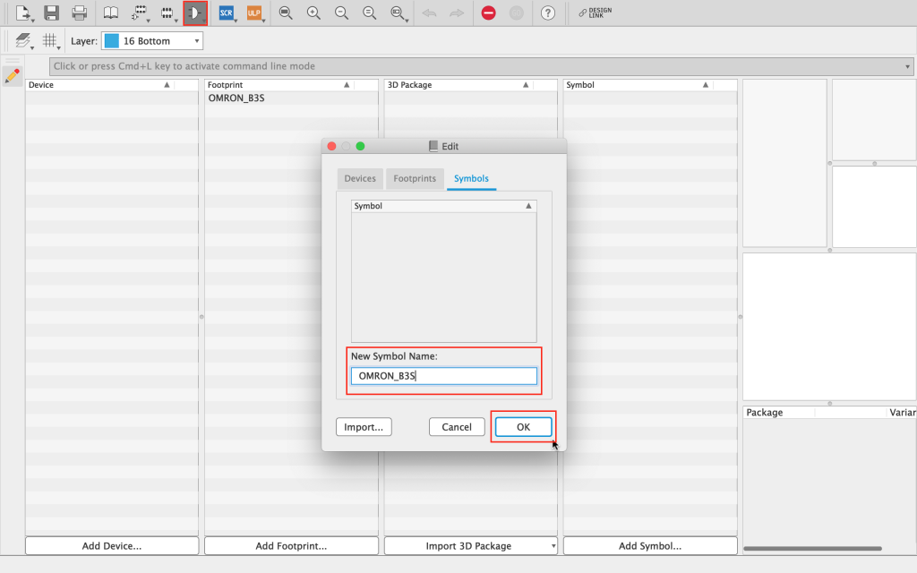
First click on the new symbol button at the top of the screen.
A dialog box will open, enter a name for the new symbol and click ok. EAGLE will ask you to confirm if you want to make a new symbol with your chosen name, click yes.
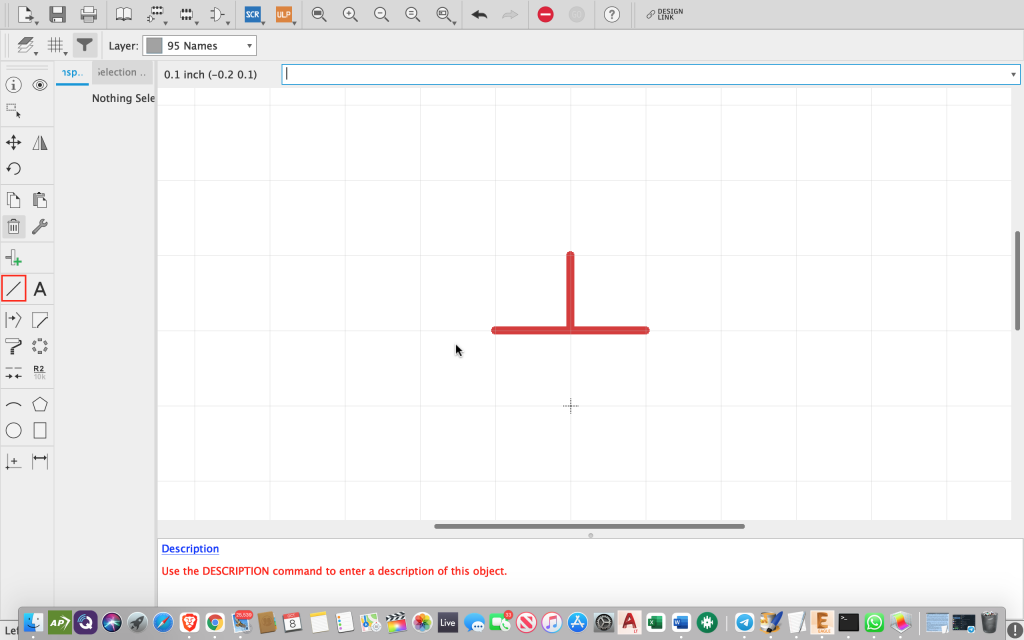
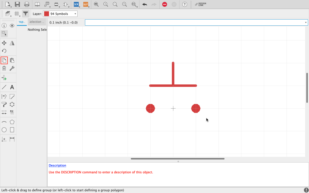
Once the symbol editor windows opens, we can begin to design the symbol. Feel free to use some of your own design creativity here, but for the purpose of this tutorial we will create a simple push button symbol.
First draw two lines perpendicular to each other just above the 0 0 (+) origin point using the line tool on the left-hand toolbar, as shown in the following screenshot.
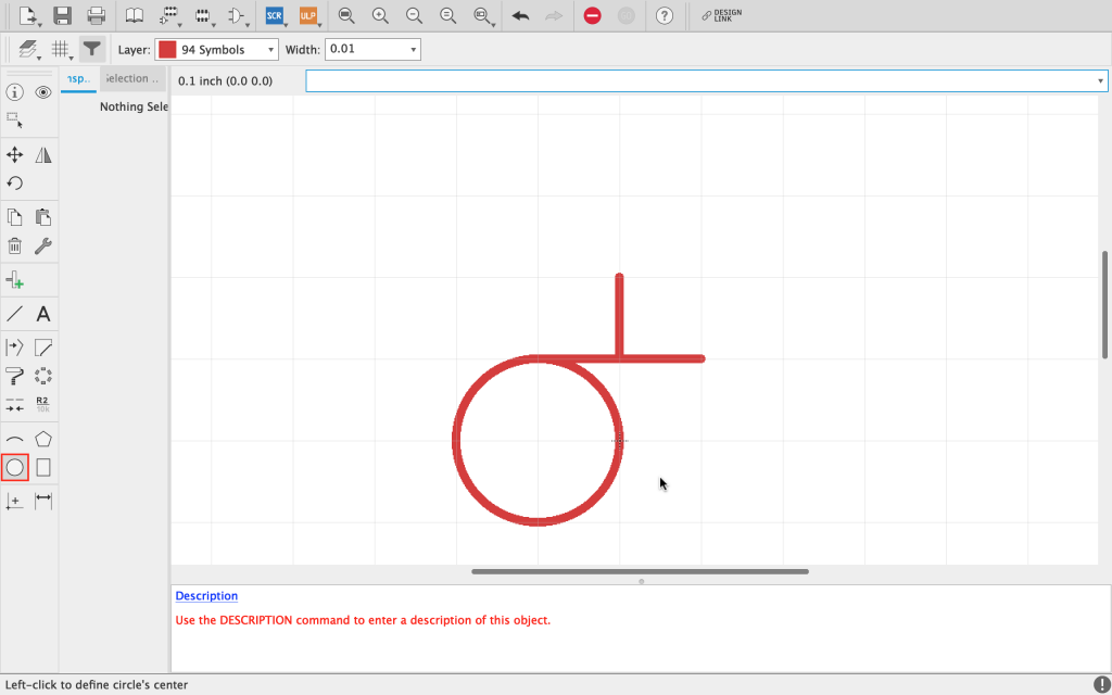
Next draw a circle at -1 0 just below the lines using the circle tool. The radius is not important at this stage as we will change it by entering the numbers directly into the properties box.
Right-click on the circle and select properties. Enter the width and radius as 0.02 and 0.01 respectively, as shown in the following screenshot and then click ok.
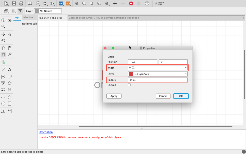
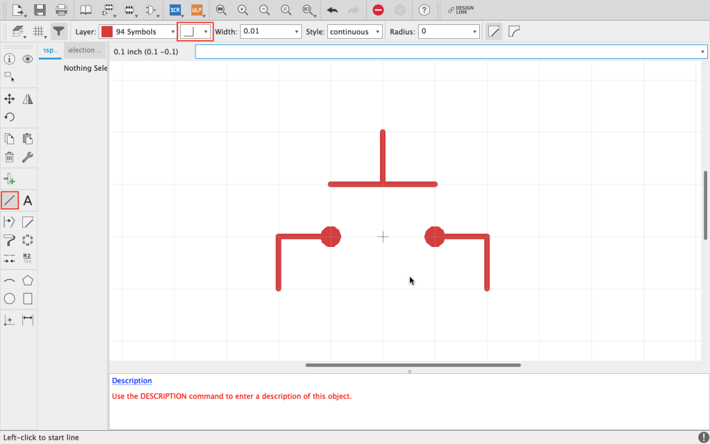
Once the properties have been manually entered, the circle will change to the desired size. Next we need to use the copy tool from the left-hand toolbar to copy it to the other side of the horizontal line.
Select the tool, click in the center of the circle and then drop the duplicate in the position as shown in the following screenshot.
Next draw two right-angled lines protruding from the circles using the line tool in the left-hand toolbar. Note that you can change the type of line using the option in the toolbar at the top of the screen.
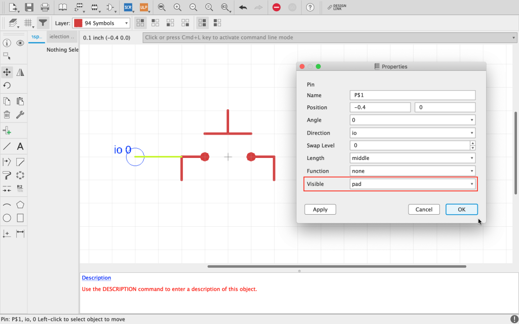
Now that we have the basic shape drawn, we need to add some pins. These are the points that will physically connect to the nets in the schematic.
If we refer back to the diagram from the datasheet, you will see that there are 4 physical pins on the switch. They are connected together in pairs to form the two switch contact terminals.
There are 4 pins simply to serve as mechanical anchoring for the component. Let’s add the first pin as shown in the following screenshot.
The green circle indicates the position where the net will connect when the component is used in the schematic.
Once the pin is in position, right-click within the green circle and choose properties. Set the visible parameter to pad in order to hide the pin label name that is cluttering up the design.
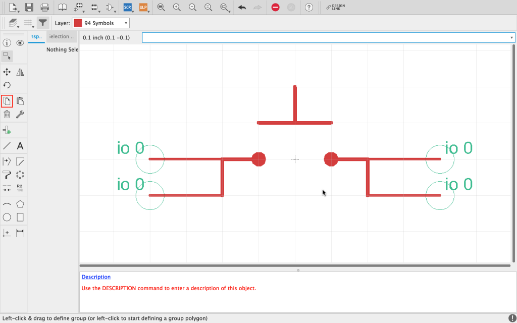
Now that the first pin is in place and the properties are set, we can use the copy tool on the left-hand toolbar to copy the pin 3 more times, as shown in the following screenshot.
Tip: you can rotate parts by right-clicking whilst you are moving them around the screen.
Next we can add the part name to the Names layer. Using the text tool on the left-hand toolbar, enter the part name in the dialog box and click ok.
Set the layer property to 95 Names and the alignment property to bottom-center on the toolbar at the top of the screen, then place the text beneath the pins as shown in the following screenshot.
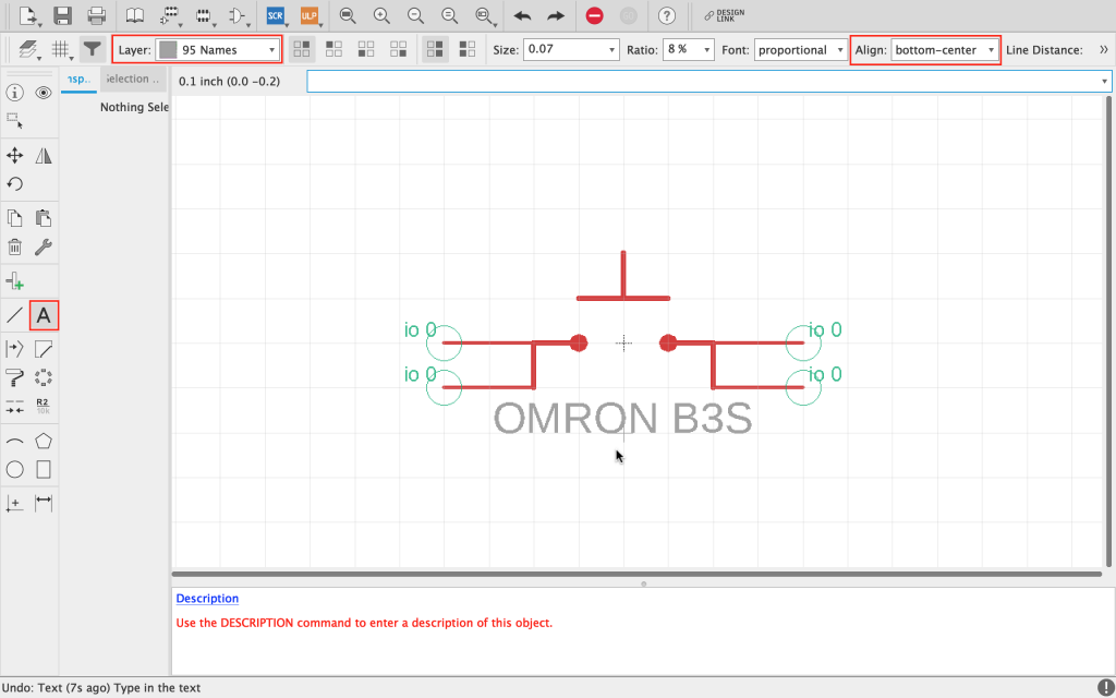
Lastly we should rename the pins to match the datasheet diagram. You will see in the diagram that pin 1 and 2 are connected together, and pin 3 and 4 are connected together.
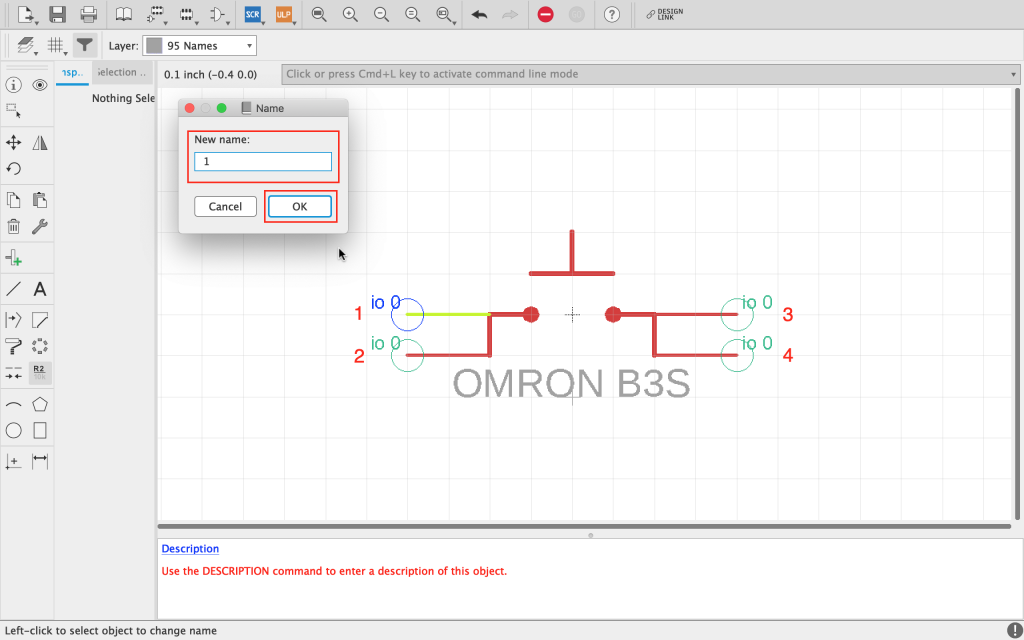
Right-click inside the green circle of the pin and choose the name tool. Enter the name of the pin in the dialog box and click ok to change it.
Rename each of the pins 1 through to 4 as shown in the following screenshot. This will make things much easier when we come to link the symbol with the footprint within a new device.
Now that we have completed the symbol design, we can save the library. Afterwards you will be taken back to the main library editor and you should see the new symbol under the list of symbols within the library.
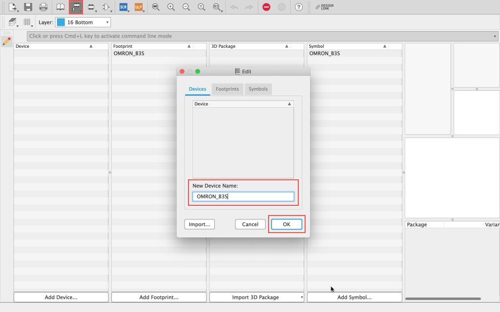
In order to link our new symbol with our new footprint, we need to create a device. This will allow us to define which of the pins in the symbol design connects with which pads in the footprint.
Create a Device
First click on the new symbol button at the top of the screen.
A dialog box will open, enter a name for the new symbol and click ok. EAGLE will ask you to confirm if you want to make a new symbol with your chosen name, click yes.
First we need to choose our previously created symbol and add it to the device design. Choose the add tool from the left-hand toolbar and select the symbol from the list, then click ok.
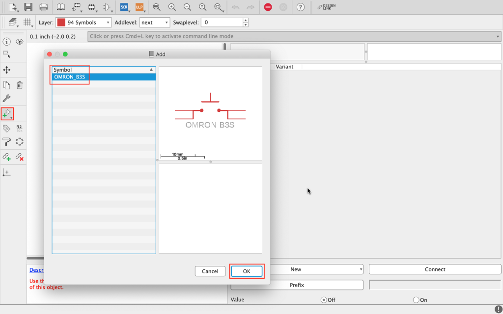
This will allow you to place custom symbol design within the work area in the same way as when editing schematic, simply move it into position and click to drop it.
Locate it with the 0 0 (+) origin point in the middle. You can choose to place the symbol elsewhere, however take note that the part will rotate around this origin.
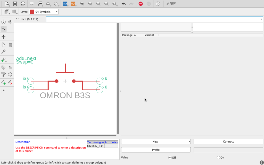
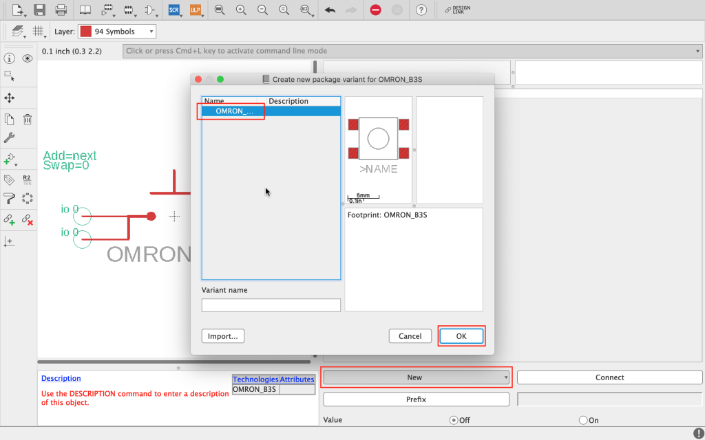
Once the symbol is in position, click the new button in the lower right-hand side of the screen to assign a new package to the symbol. Select the option to add a local package.
It is possible to assign multiple packages to one symbol, which is useful if there are multiple package variants available for a component. However in this example we just need to assign the single package that we created.
A dialog box will open with a list of packages in the library. Select the previously created package and click ok.
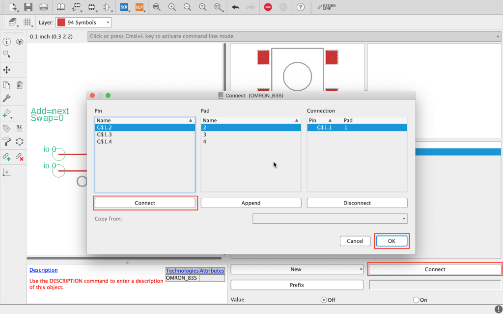
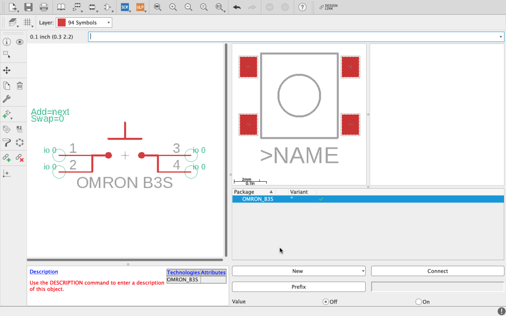
Now you will see the package appearing in the main device design window, however the small warning triangle indicates that there are missing connections.
Therefore next we need to assign the pins in the symbol to the physical pads in the package. To do this, simply click the connect button to bring up the connect dialog.
You will see the pins and pads from the symbol and package in the pin and pad lists. When clicking the connect button, the selected pin will be connected to the selected pad.
First select pin 1 and pad 1 from the lists and press the connect button. You will see a connection created in the connections list box. Repeat this for pads 2 through to 4 and then click ok.
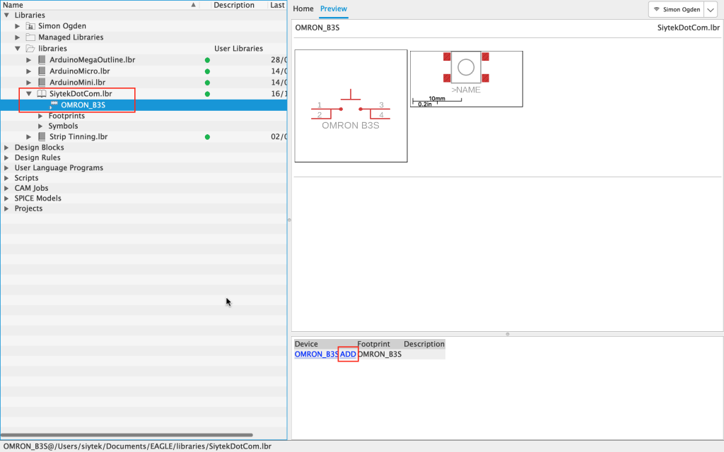
Now that the connections are made, we can save the library and our new component is ready to use!
Placing a Custom Device Into a Schematic
Now that we have completed our custom library and component, we will add it to a schematic.
For this example we will use the schematic created in the previous tutorial. However if you are not following the entire series then you can still use this as a guide to add the custom component to your own design or a blank schematic.
First we need to open our schematic if it is not already open.
Once the schematic is open, select the add part tool and you should be able to locate your newly created library component! Awesome!
Click ok and you will be able to drop it into the schematic like any other component.
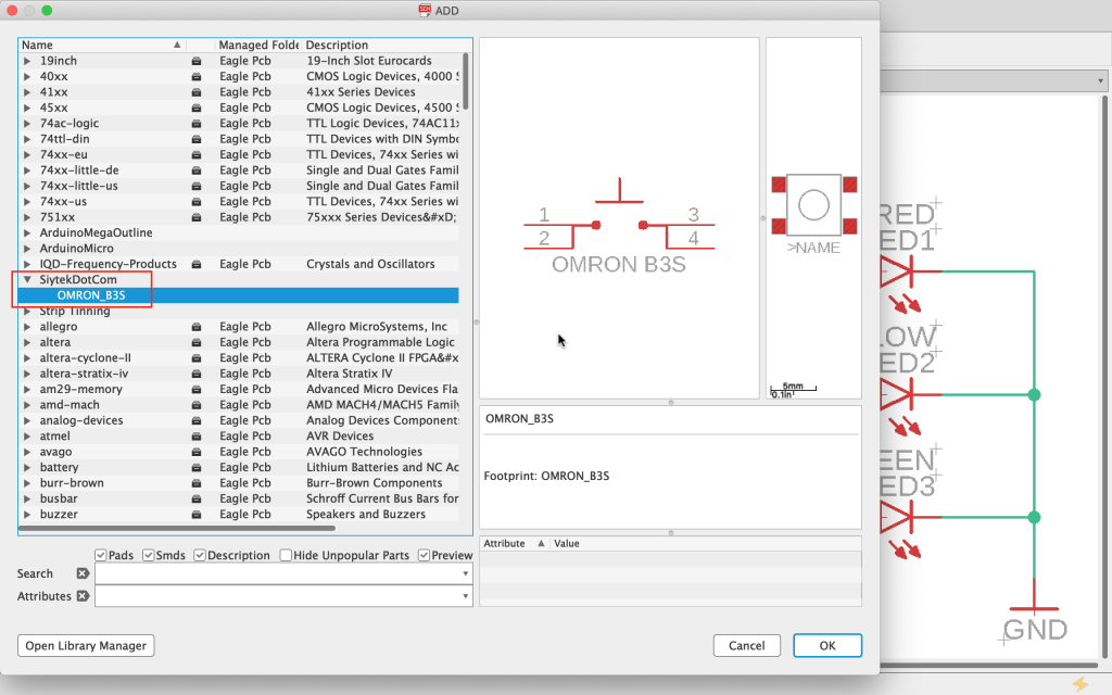
It is worth mentioning here that I have had problems in the past, particularly with Windows based versions, whereby the library was not visible.
First you can try saving everything, then close EAGLE and try again. If that does not work then you can add the component from the main EAGLE welcome screen, as shown in the following screenshot.
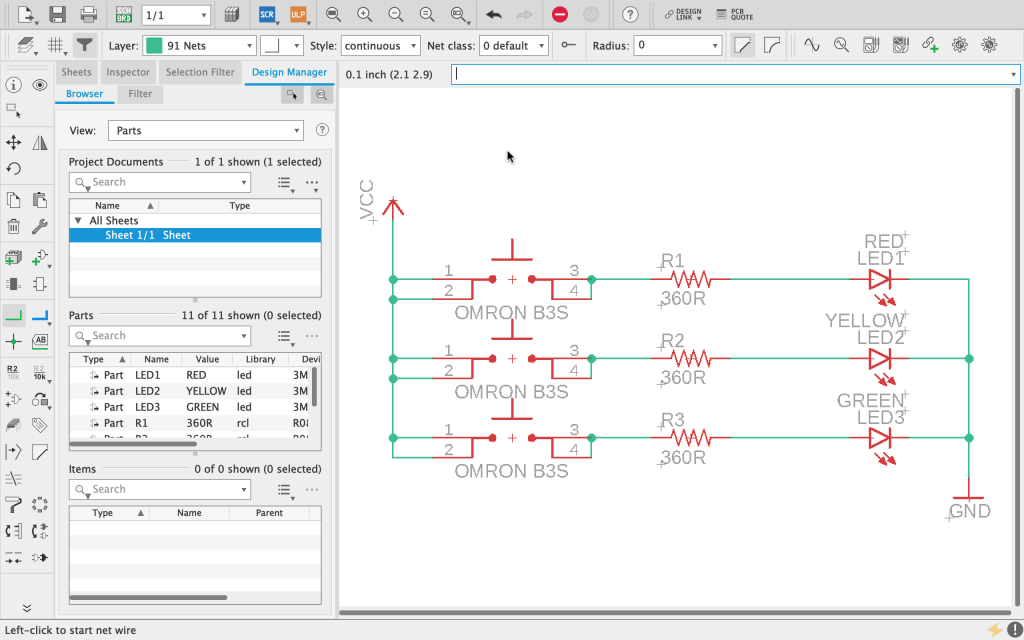
Once you have your custom component within the schematic, if you are working through the tutorial series then you can complete the schematic from the previous tutorial by placing three B3S switches into the design and connecting them as shown in the following screenshot.
What’s Next…?
A big well done for getting to the end of the tutorial! So far in the series we have covered the basics of getting started and making a schematic, followed by how to add a basic library component.
In later tutorials we will cover some of the more advanced tools. These are useful for more complex designs and also for speeding up your workflow.
Now that we have a completed schematic, it is possible to progress on to the board design itself.
EAGLE keeps the schematic and board design in two distinctly separate environments, each saving files into its respective .sch and .brd formats.
When both files are opened simultaneously, EAGLE will keep them synchronized and it is important to keep both files open together to maintain congruence.
In the next article we will get stuck into the board editor and walk step by step through the process of designing a simple PCB from our previously created schematic.
Check out the next tutorial in the series… EAGLE CAD Board Layout Tutorial (Easy Dummies Guide!)
Thanks so much for visiting my site! If this article helped you achieve your goal and you want to say thanks, you can now support my work by buying me a coffee. I promise I won't spend it on beer instead... 😏