Don’t you wish that sometimes you could sit down and ask a PCB process engineer “what is the ultimate secret to making a PCB the cheapest it can be?”
After spending over a decade working in high-tech PCB facilities, I wanted to share with you my 7 top tips on how you can get the most from your PCB supplier!
Want to know the best place to go for a great value PCB? I am currently recommending this place!
With that said, here are 7 expert PCB tips from a former PCB Process Engineering Manager…
Are Single Sided PCBs The Cheapest? The Answer Will Surprise You!
One might be inclined to believe that a single layer board is the most economic.
This is not actually always true.
For example, take a look at this quote from PCBWay for a double-sided board:
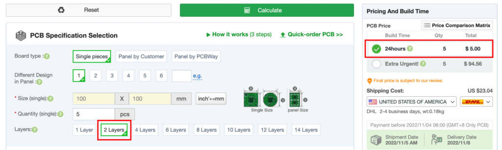
We have a 2 layer board selected and the price currently quoted is $5 for 5 boards.
Now look what happens when we change the number of layers to a single layer…
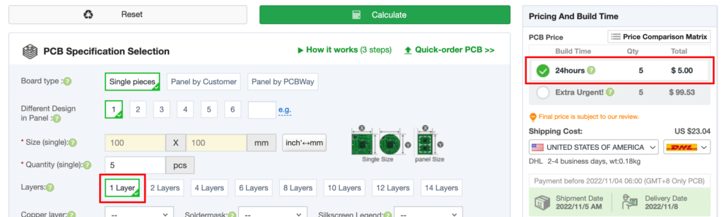
Here you can see that the unit price is exactly the same.
None of the other features have been changed, all we did was change to a single layer.
Not only that, but the eagled-eyed amongst you will have noticed a slight increase in price for the extra urgent delivery.
This suggests that a single layer board and double layer board have the same cost to manufacture. There are several reasons for this:
- A single layer board still needs pads on the bottom side in order for the plating process to plate the holes through. This means as far as the factory is concerned, a single layer board is basically just a double layer board with no tracking on the bottom.
- If you don’t wanted the holes plating through, producing a single layer requires a different process route. It is not worth changing the machine configurations just to produce a small quantity of single layer boards.
- Materials are usually copper clad on both sides. Your single layer board will still need all of one side etching off, costing about the same in chemistry.
- The laminator will still laminate both sides of the panel, costing the same in photo-resist.
- The solder mask curtain coater will still coat both sides of the board with solder mask.
- It is way more common for a PCB fabricator to process double-layer boards. This makes it far more economical for the fabricator to panelize your job with other double-layer boards, regardless of whether it is one or two layers.
The takeaway here is that double layer boards are the most economical choice.
You get the most real estate for circuit tracking and it simplifies your design, therefore you will save time (and therefore money) when designing the PCB.
What about going in the other direction?
Making the PCB a multi-layer (4 layers and upwards) will introduce a whole host of new processes, such as bonding.
Therefore there is a big jump in cost between a double sided PCB and a 4 layer as you can see here:
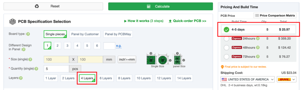
As you can see we are looking at 5 times the price for 5 units!
This is due to all of the extra processes and considerations that are required for a multi-layer board, but we won’t dive into that too deeply here.
Choose The Right PCB Material for the Most Economic Quote!
Now that we understand that the most economical choice for manufacturing a PCB is to make it a double-sided design, what about material choice and thickness?
Most PCBs are manufactured from FR4, which is fibreglass.
The only instances whereby you may deviate from this is if you are making something very specialist, where cost would not be so much of a consideration!
Fabricators will likely keep a large stock of the most commonly used materials.
You will find many different types of FR4 available, primarily different thicknesses but also with a different glass transition temperature, also known as Tg.
As our economic design is a single layer and will not be put in a heated press for bonding, we are not too concerned about glass transition temperature.
Therefore the material we need to use is the standard Tg and standard thickness offered by the fabricator, assuming your design does not have constraints for PCB thickness.
This is most likely to be 1.6mm FR4 with a Tg value of approximately 150C.
Let’s take a look at the pricing over at PCBWay. This time I have tabulated the data for clarity.
The table shows the price for 5 PCBs with different thicknesses and Tg values:
| Thickness (mm) | Tg 130-140 Cost ($) | Tg 150-160 Cost ($) |
|---|---|---|
| 0.2 | 96.80 | 96.80 |
| 0.3 | 96.80 | 96.80 |
| 0.4 | 96.80 | 96.80 |
| 0.6 | 5.00 | 5.00 |
| 0.8 | 5.00 | 5.00 |
| 1.0 | 5.00 | 5.00 |
| 1.2 | 5.00 | 5.00 |
| 1.6 | 5.00 | 5.00 |
| 2.0 | 97.30 | 66.61 |
| 2.4 | 67.89 | 67.89 |
| 2.6 | 126.80 | 128.57 |
| 2.8 | 126.80 | 128.57 |
| 3.0 | 127.55 | 129.08 |
| 3.2 | 127.55 | 129.08 |
Note that in most cases, PCBWay upgrade from lower to higher Tg for free. Therefore the economic pricing shown here is likely all for the more commonly stocked 150-160 Tg material.
The table shows that the most economical choice is to use a 150-160 Tg FR4 material and maintain a thickness of between 0.6mm and 1.6mm.
The reason these certain materials are so much cheaper, is because they are commonly being processed.
All of the processes are set up to accept these material thicknesses.
Most designs processed by the fabricator are using these thicknesses, therefore your design can easily go on to a panel that is already in production.
This makes it hugely more economical to produce your PCB.
Stick to the common material and most common thicknesses in order to get the most economic quote!
Hole Size Matters, Not Too Big, Not Too Small for Economic PCB Drilling.
Imaging for one moment, a state-of-the-art PCB drilling machine.
These machines drill thousands and thousands of holes. Panels are loaded in and the drill heads seemingly pound the material like a machine gun!
Each drill can have a certain amount of wear and tear before it starts to produce poor quality holes.
Many drills must be kept in cassettes so that the machine can index to another, and another, and another as the drill bits wear out.
There is only so much room in one of these machines for drill bits.
Therefore there are two things that can be done to make the process more economical:
- Use a fewer number of holes (vias) in your design.
- Use as fewer different hole diameters as possible.
When you optimise your design to have less vias, the drill program time can become a lot shorter.
Time is money in manufacturing and a shorter program time equals direct savings for you.
Another top tip is to merge component hole sizes.
Often in your design library you might find one component has a 3.1mm hole and another a 3.176mm hole. Change the 3.176mm holes to 3.1mm!
This means the drilling machine has to perform one less tool change, making it quicker, saving you money!
It is also worth saying that in both cases, machine stoppage time is also reduced.
Less holes equals less wear on the tools, which means more panels can be processed before an operator must stop the machine to replace blunted drill bits.
Also, the fewer amount of different diameters you need to keep in a cassette, the more space you have for additional drill bits in the size you choose to stock in the machine.
The more stock of drill bits you have loaded in a particular machine, the longer it can drill for without being stopped by an operator to replace blunted drill bits!
The take home here is a fewer number of holes and fewer diameter variations in your design will be more economical.
But what about maximum and minimum size?
I have seem drill diameters down to 0.15mm and I know that is not even the smallest!
If you have never seen a 0.15mm diameter drill bit before, it looks a little like a tiny hair. The lightest touch will snap it!
It is also true to say for a 0.2mm diameter.
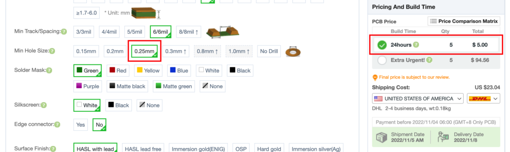
However things start to get a little easier at 0.25mm. In PCB manufacturing, this drill diameter is where you start to see less problems.
This is evident when looking at the PCBWay quotation. A minimum hole size of 0.25mm and above gives us the economical price of $5 for 5 PCBs.
We can see a dramatic difference when dropping the minimum hole size to 0.2mm or less!
Now the price has shot up to $66.35 for 5 PCBs, a dramatic difference!
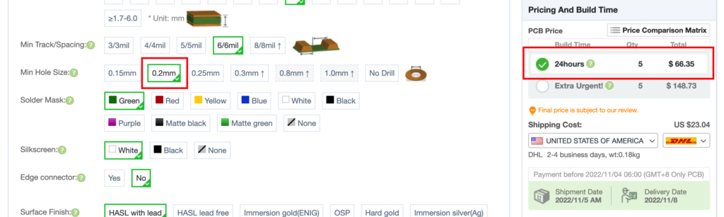
There could be multiple reasons for this. Most likely the panel needs to go on a specialist machine that is capable of drilling the smaller sizes without causing scrap.
When I worked as a drilling operative many moons ago, we had 10 machines and only 2 of them were capable of drilling 0.2mm holes and lower consistently, without causing scrap.
Personally, for the most economical design, I would keep hole sizes to 0.3mm and above, unless you absolutely have to reduce them.
On a final note you should also be aware that there are recommendations for maximum hole size too.
Here’s a little insider tip…
Holes that are smaller than 6.0mm can be tented by dry film resist.
These holes can be drilled at the same time as the plated through holes (PTH).
You can put them in your PTH program, and then specify that they are non-plated (NPTH) in a drawing.
So long as you do not have copper pads on these holes, they will covered with dry film and won’t be plated.
Putting your < 6.0mm holes in your PTH drilling program, as NPTH holes, means you do not need a second strage drilling process for NPTH holes.
Of course, omitting one drilling process should save some cash!
For holes > 6.0mm, you can move them to your routing program. These holes will then be routed just prior to the board profile.
PCB Profile Routing Can Often be Made More Economical
I remember working as a CAM engineer, when one of the process engineers came storming up into our office complaining about an impossible 40um track and gap that he could not etch.
We opened the data and we started laughing.
In a frustrated tone of voice he asked us what we were laughing at.
I turned the computer monitor round, displaying the track in the design data and told him, “looks fine to us.”
Often it is easy to get carried away when working in the virtual environment. Designers create beautiful PCB profiles, with carefully crafted contours and curves.
However it is easy to forget that profile routing can be one of the most time consuming processes in PCB manufacturing.
There are two optimisations that can dramatically reduce this time, and as we know in manufacturing, time is money!
- Optimise your data.
The CAM engineering process it not perfect. If you supply a curve in your profile as thousands of tiny little lines, rather than a geometric arc, it can take the machine notably longer to cut.
These optimisations often can get missed. Lazy CAM engineer (I have been that guy). Even the software didn’t catch it or optimise it properly.
Make sure the data that you are supplying is clean and you are more likely to get top results on the factory floor.
- KISS – Keep It Super Simple!
It goes without saying that a rectangular PCB will rout much quicker than something with a lot of complex geometric shapes.
Not only will a rectangle produce a much quicker rout program, it will also tessellate into a PCB manufacturing panel, which for sure will save you money!
Another thing to remember is that a round tool cannot cut a square.
Routing is carried out by a round tool that rotates at high speed. The tool is plunged into the manufacturing panel and then moved to cut around the profile of your PCB.
In which case, the tool always ends by leaving a half-circle, equal to the diameter of the tool.
Whenever the tool changes angle, a radius is left. When the tool changes direction 90 degrees, a radius equal to the radius of the tool is left on the outer edge.
This of course only applies to inside edges.
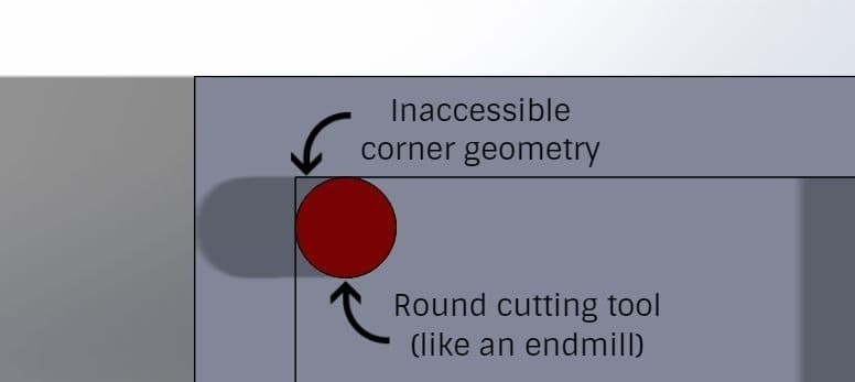
The PCB fabrication will likely have a preferred or most common tool diameter for ‘run of the mill’ cutting.
Commonly a 2.0mm mill bit.
When you design your board profile, if you have any internal corners, ensure that you use a radius equal to the diameter of the fabricator’s most commonly used end mill.
If in doubt, just use a 1.0mm radius (for a 2.0mm routing tool).
Also, if you are designing your own array/biscuit of multiple circuits, take this into account when you are spacing them.
Unless you are planning to V-cut, you need to space the circuits at least about 0.1-0.5mm further apart than the diameter of the most commonly used mill bit.
Conclusion
If you made it this far, well done!
Optimising PCBs is certainly not a trivial topic and far extends beyond what has been discussed here.
However some of the more important considerations have been discussed in this article and I hope you will save a little money as a result!
If you are looking to get some PCBs manufactured for a great deal, even if you only want a few prototypes, be sure to check out these guys!
Thanks so much for visiting my site! If this article helped you achieve your goal and you want to say thanks, you can now support my work by buying me a coffee. I promise I won't spend it on beer instead... 😏