Whether you are designing a PCB, getting a PCB manufactured or planning to do a bit of DIY PCB manufacturing, it is vital to have a good understand of PCB layers.
After working in the HDI and Flexible PCB manufacturing industry for over a decade as a CAM and process engineer, there isn’t much I can’t tell you about PCB layers!
Understanding what the different layers are and how many you should include in your PCB design is absolutely necessary,
And guess what…?! It can even save you a whole bunch of money!
In this article you will learn many of the important fundamentals about PCB layers, which will no doubt aid you in both PCB design and PCB manufacturing.
What Are PCB Layers?
There are two terminologies that you might come across when investigating PCB layers.
Firstly, we can discuss the number of layers in a board design. Here we are generally referring to the number of copper layers in the design.
A PCB can be single copper layer, double sided (a 2 layer board) or multilayer.
I have personally worked on PCBs for Intel, which had 30+ copper layers!
Secondly, we can discuss the types of layers that are involved in a PCB design. The main layers of interest are as follows:
- Silkscreen – this is the (usually) white print on top of the PCB, which indicates component placement and other information, such as manufacturing date and serial number information. It can also include a company logo!
- Soldermask – this is where PCBs get their distinctive ‘green’ color, although nowadays many different colors are available. The purpose of soldermask is to isolate and protect all areas of the PCBs that do not need to be exposed (for soldering).
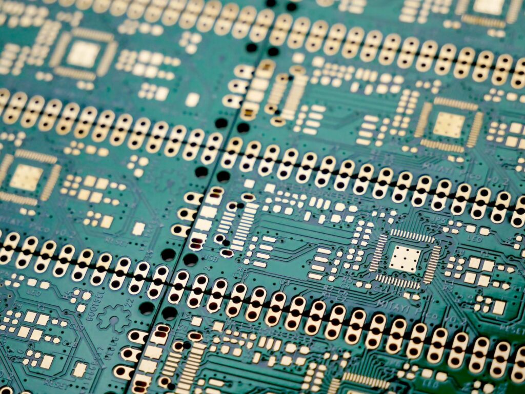
- Copper Layers – these contain the conductive part of the design, things like your copper tracks, pads, component footprints and ground planes.
- Drilling – there can be various layers for drilling, containing plated holes, non-plated holes and holes that are to be drilled through different parts of the stackup (the arrangement of layers).
- Routing/Mechanical – usually containing the outline of the circuit, including any internal cutouts. Multiple rout layers may also be used to create things such as plated edges, or holes that are too large to be drilled.
- Pick and Place – used for PCB assembly and contains all of the component center coordinates. This is the place that the pick and place machine will place the component on the PCB during assembly.
- Drawings – it is not always necessary to produce a drawing in order to get a PCB manufactured, but it can help the fabricator. With that said it is necessary to produce a drawing if your design requires anything a little unorthodox.
We will discuss these further later in the article.
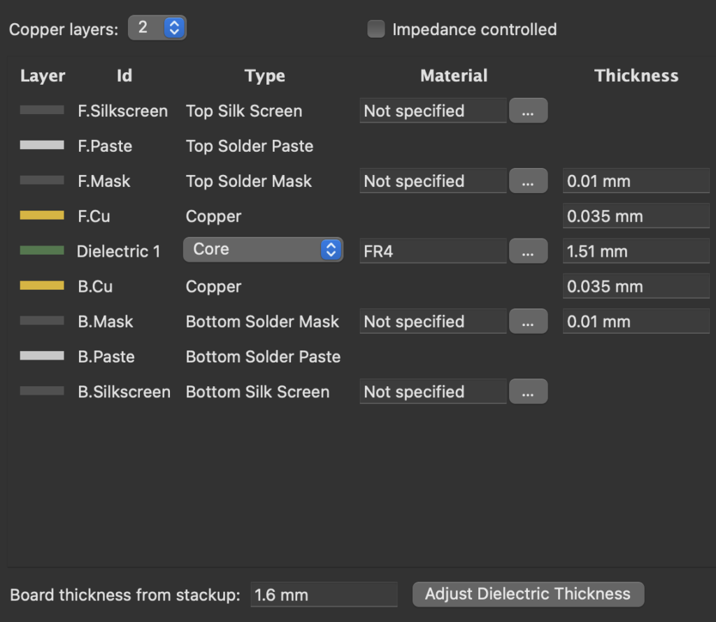
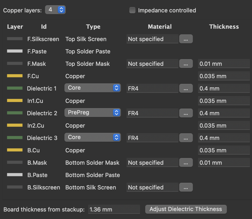
What is a 2 layer and 4 layer PCB?
A 2 layer and 4 layer PCB is a printed circuit board that consists either of 2 or 4 copper layers respectively.
If you are a maker or DIY enthusiast looking to produce your own PCBs then chances are you will be considering either a 2 or 4 layer board for your design.
Confused?
Alternatively you could think of it more like this…


I have already explained why it is better to design a 2 layer board, rather than try to squeeze a design on to a single layer.
You can read more about why I recommend double-sided boards here.
It can also be a be quite a bit more expensive to jump from a 2 layer board to a 4 layer board, due to the additional processes required, such as lamination.
A double-sided board is the best choice for many DIY enthusiast projects. However here are some reasons that you might consider a 4 layer board:
- If you have a space or weight critical design, a 4 layer board can save considerable real estate. Your PCB design can be reduced in footprint a notable amount.
- If your design has a lot of complexity and requires a lot of signals (high numbers of bits digital buses for example), it may be necessary to go up to 4 layers.
- If your design has sensitive analog circuitry, it may be preferable to include an internal copper plane and avoid running power traces all over the place, in order to reduce noise.
- If your design requires impedance matching for high speed signals or an RF application, it may be necessary to include internal planes.
Can A PCB Have 3 Layers?
Yes, a PCB can have 3 layers. However there are a number of reasons that it is advisable to avoid a 3 layer design.
- PCB materials usually come clad with copper on both sides. Therefore when using commonly available materials, a stackup will always have an even number of copper layers.
- If a 3 layer design was manufactured, it is likely that it would be manufactured as a 4 layer PCB with one blank internal layer. The cost would therefore be the same as manufacturing a 4 layer board, which means you may as well design it with 4 layers.
- A 3 layer board could be manufactured with an uneven stackup, for example a double sided board with a copper foil bonded on one side with a dielectric separator. The problem here is if the stackup is not even, the board will often bow during bonding. We call these ‘banana boards’ in the lamination department! They need additional baking to be flattened.
The takeaway here is that a 3 layer design is more trouble than it is worth.
It is actually cheaper and easier to just produce a 4 layer board with standard materials and manufacturing processes.
What Are The Different Types of PCB Layers?
At this stage you should have a basic understanding of what is involved in a PCB stackup.
Let’s take a more in depth look at the different types of layers that are required in order to manufacture a PCB.
Soldermask
The soldermask layer is placed on top of the copper layer once it has been deposited.
This gives the PCB its green color and serves as insulation for the copper layer, preventing it from coming into touch with any other metals or board components that can damage the copper traces.
This layer aids the user in soldering in the proper locations, which is crucial for the manufacturing process when the components are attached to the board.
Silkscreen
The name ‘silkscreen,’ like many things in PCB manufacturing, comes from the historical name of the actual process used.
By putting letters, numbers, and symbols to the board, the silkscreen primarily serves to aid us humans in understanding the board and the operation of certain pins or LEDs.
We also call this the ident layer, short for component identity.
In the past we used to use the same silkscreen printing process that is used in textiles, in order to print necessary human-readable information on to PCBs.
We also used this process to print the aforementioned soldermask on to PCBs. You can even print and etch the copper using screen printing.
This is the original reason it is called a printed circuit board!
Large scale fabricators have mostly abandoned screen printing in favor of more modern methods, which was driven by advances in technology.
The only areas where I have actually seen ‘printing‘ used in printed circuit manufacturing is for printing the ident layer on the board, and only when an unusual color was requested.
For the 99% of boards that required white ident, a machine was used that could be likened to an inkjet printer on steroids!
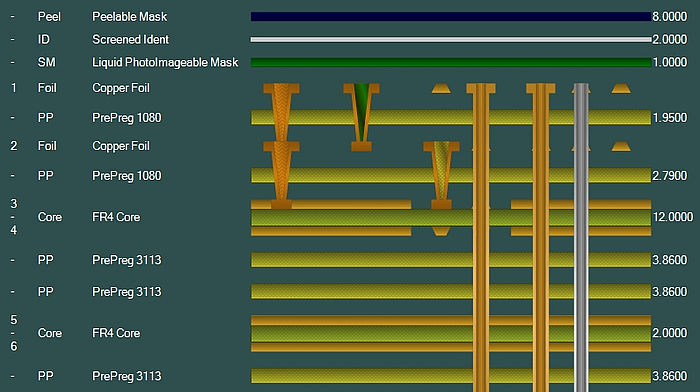
Copper & Dielectric Substrate
The copper layers are the ‘meat and potatoes‘ of the PCB.
When we think of a circuit board, we think of the iconic traces and pads pattern. Beneath the soldermask lies the etched copper traces that make the magic happen.
Although the technology has changed dramatically over the decades, the process of producing the copper design remains fundamentally the same.
We begin with a solid copper foil attached to a dielectric (non-conductive) material, most commonly fibreglass.
We then use some wizardry to convert our PCB design into an etch resist, which is transferred to the copper foil.
Finally we douse the panel with a series of chemicals, which dissolve away the exposed copper and then remove the protective film.
What we are left with is our circuit design in copper, ready to be covered with solder mask.
There are some other more elaborate ways to perform this process, such as by using an additional tin plate to act as the etch resist instead of the dry film or ink, but that is beyond the scope of this article.
Drilling
In its most basic form, drilling is rather self-explanatory.
Mostly all PCB designs require drilling in order to connect the top, bottom and internal layers, if applicable.
Traces on different layers can be run to a pad, a copper circle that will have a hole drilled through it.
The hole to be drilled will be smaller than the copper pad. The amount of copper remaining (think of a donut) is called the annular ring.
The barrel of the hole is then copper plated, which connects the pads and allows electrical connections to traverse between layers.
We call this a plated through-hole, which we refer to as a PTH.
Note that we can also drill non-plated holes, which we call a NPTH. These holes are usually used for mechanical fixings etc.
Mostly all PCB designs will have at least one drilling layer. This layer contains all of the hole sizes and positions to be drilled.
Things can get complicated pretty quickly though!
Multi-layer circuits can have all sorts of configurations. For example a 4 layer board can have two drilling layers.
The first drilling operation is carried out on layer 2 to layer 3, which it still exists as a single core material.
Once the drilling, etching and plating has been completed. Two additional foils are bonded on to form layer 1 and layer 4.
The second drilling operation is then carried out, connecting layers 1 through to 4.
Confused yet?
This is just the start of it! However this is beyond the scope of this article and deserves its own article entirely!
Routing/Mechanical
When manufacturing PCBs, the fabricator will begin with standard sized material.
The size of a “manufacturing panel” can vary a lot. Personally I have used 24″ x 18″ size most commonly, plus 12″ x 18″ and even down to 9″ x 12″.
However this was producing complex products that were quite difficult to manufacture. I am talking about small and medium volume high tech stuff, and some top secret prototypes!
If you head east to the facilities that mass produce consumer goods, the panels can be upwards of 60″ in length!
In any case, your circuit design will be produced in a much larger “manufacturing panel” and at the end of production, must be cut from this panel so that it can be shipped to you.
This is where the routing layer comes in.
The rout layer in your design usually features just the board profile outline. It can also feature any internal cutouts that you may require.
During the CAM engineering process, information is added that compensates the tool path.
In order to cut the outline specified in your routing file, the machine will be using a round tool, for example with a 2.0mm diameter.
Therefore the machine must cut with the tool 1.0mm (the tool radius) over to the side, so that the edge of the tool is cutting the line that you have drawn.
If no compensation is applied and you cut directly down the line in your design with a 2.0mm tool, your board will be 1.0mm smaller all of the way around!
If that was a little tricky to grasp, here is a great video that explains the principle:
Conclusion
If you have made it this far, congratulations!
In this article we have covered some of the basic yet crucial information that needs to be understood about PCB layers.
I hope you have learned something more about printed circuit boards! Now unless you like wasting money, I would suggest you read this PCB article!
Thanks so much for visiting my site! If this article helped you achieve your goal and you want to say thanks, you can now support my work by buying me a coffee. I promise I won't spend it on beer instead... 😏