
So you got yourself an Intel FPGA, loaded Quartus and then had a meltdown because of the sheer volume of things to click on the screen, right?
Fear not my friend, I have been there too.
This guide will have you programming that slick looking FPGA in no time!
This guide aims to cover some of the staple parts of Quartus, including how to create a project and how to use the pin planner to link your design to the hardware.
We will also walk through the process of how to program the FPGA with the programmer.
As this is a complete beginners introduction to Quartus, we don’t need to write any code just yet as we will only be using the simple logic functions built into Quartus.
Don’t worry if you are still trying to decide whether to join the SystemVerilog or VHDL camp, this tutorial is a great prerequisite for either.
- Prerequisite
- Create a new project
- Building a logic circuit
- Configure the hardware
- Compile and program the FPGA
- Conclusion
Prerequisite
You will of course need to have Quartus Prime installed and running on your system. If you are using Windows you can just go ahead and download it once you sign up for a free Intel account.
If you are using Linux then you can also download the Linux version.
There is however some additional setup required to get the USB-Blaster programmer to work. You can check out this information for more details on how to get the programmer to work.
If you are using Mac then you can run either the Windows or Linux version of Quartus Prime in Virtualbox.
My preference would be to use the Linux version and you can go ahead and check out my tutorial on how to set it up if you would like to install Quartus Prime on Mac.
Lastly you are going to need an FPGA to program!
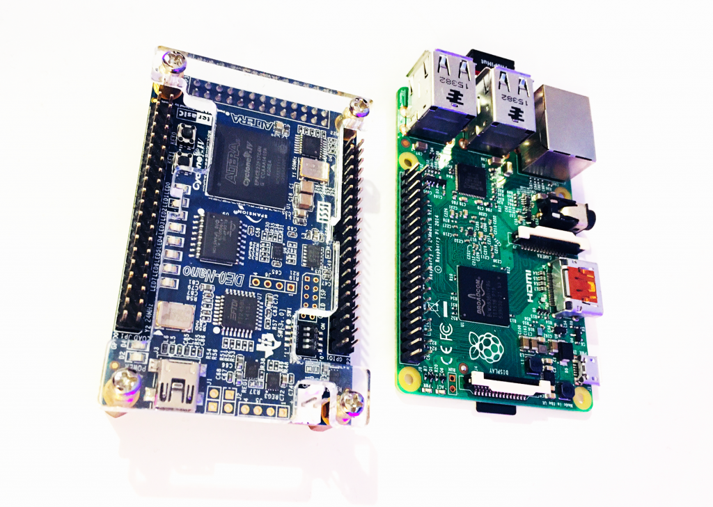
Personally I like using the Terasic DE0-Nano as it is slightly smaller than a Raspberry Pi and has many awesome features. This means I can lazily sit back on my sofa and write code whilst having an awesome feature-rich FPGA board to hand.
Create a new project
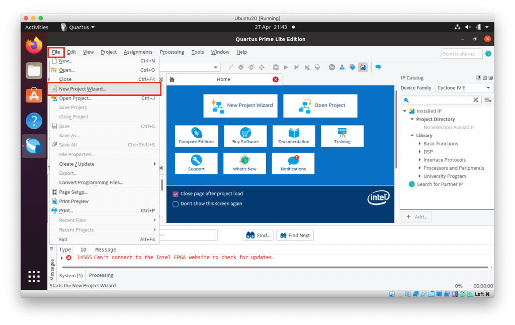
Creating a new project in Quartus is really easy, despite the plethora of menu options thrown at you. Go ahead and click file > new project wizard… to begin the new project wizard.
Setup the project
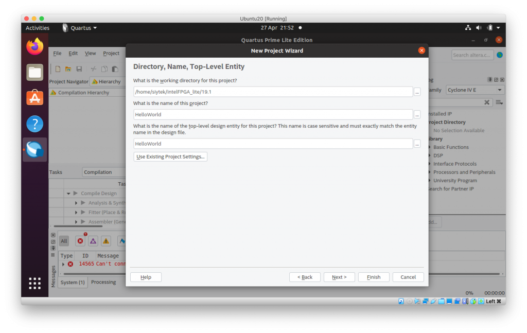
The first page of the wizard is a brief introduction that you can skip past. On the next page you can go ahead and enter a path for your project as well as a project name.
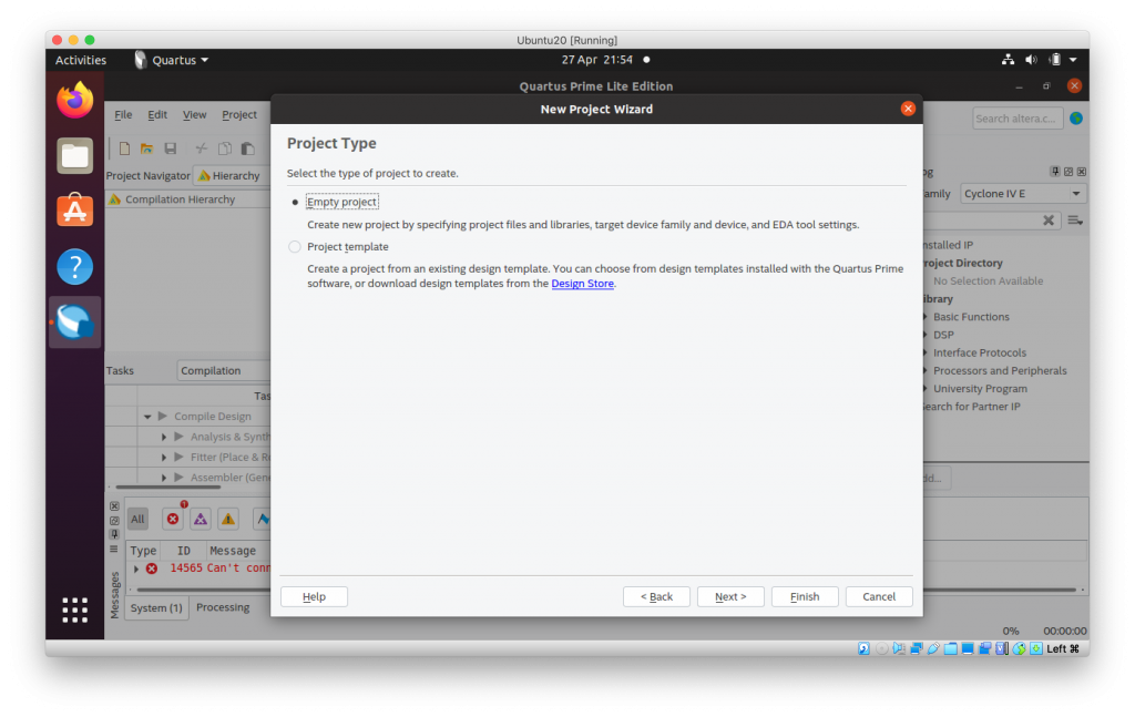
On the next page choose an empty project.

For this project we do not need to add any empty files. However for future projects, this dialog gives you the opportunity to include any design files from the start.
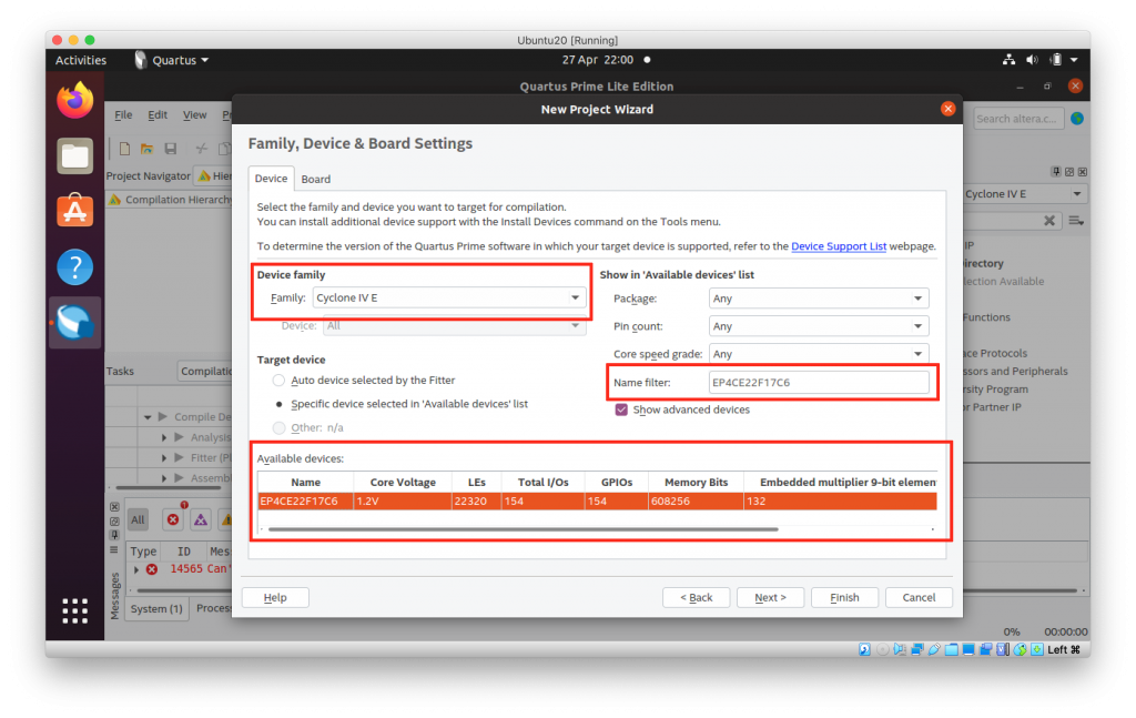
Choose your device
Next we need to choose our device, more specifically the FPGA chip that we are using.
This information will likely be printed right on top of the chip so long as you can see it.
You could also find it in the technical documentation for your particular development board.
The DE0-Nano uses a Cyclone IV series FPGA and the model is EP4CE22F17C6.
We can enter this information into the device family drop down box and then filter by name. Once the device appears in the list at the bottom, we can highlight it and click finish.
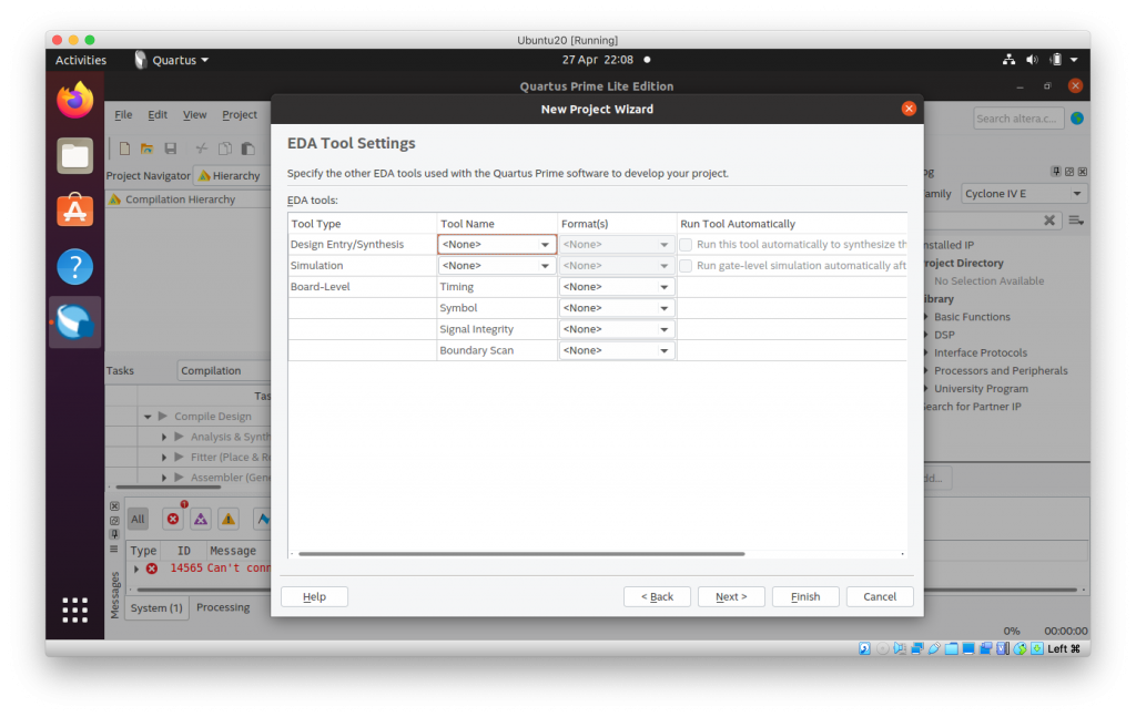
Choose EDA tools
For this introduction to Quartus we will not be writing any code, therefore we do not need to use any EDA tools for this project. Just leave everything set to the default and click next.
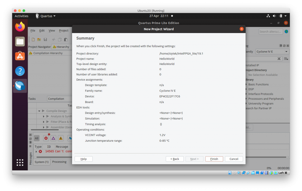
Completing the wizard
Lastly we will be presented with a summary of our project setup. Feel free to take a look and check if everything looks correct, then click finish to complete the wizard.
Building a logic circuit
Once we have completed the wizard we will be taken back to the main Quartus screen, now without the welcome splash screen.
We are now ready to start building our first project. Awesome!
In order to demonstrate some of the staple features of Quartus, we will build a very simple logic circuit that links a pair of physical inputs to a physical output on the chip.
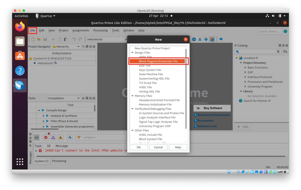
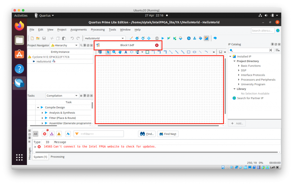
Create a new block diagram
Go ahead and click file > new… to open the new file dialog box. We are going to create our first block diagram/schematic file, simply select it from the list and click ok.
You should notice that we now have a new file in the tabs at the top of the work area. This new file will present us with a grid-type layout area where we can draw schematics.
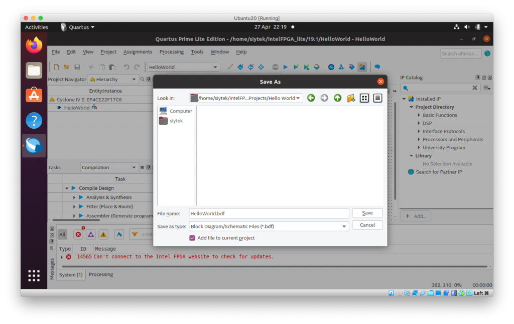
Save the block diagram
You might want to go ahead and save the file at this stage, click file > save as… and then give your file a name, choose a suitable path and click save.
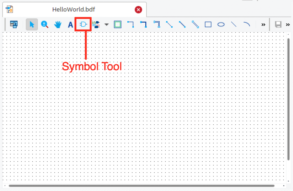
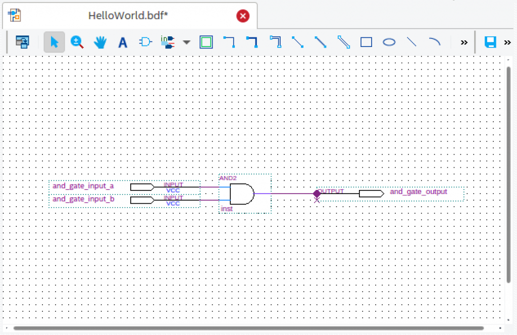
Creating logic
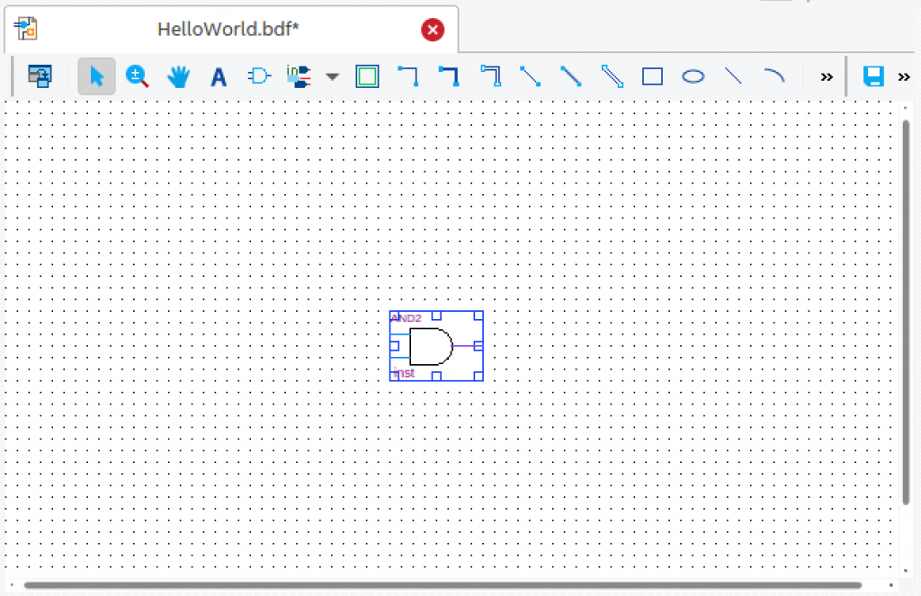
First we will add a simple AND gate to our design. In order to add a symbol from the library, go ahead and click the symbol tool from the tool bar at the top of the workspace.
This will open the symbol browser where you will notice three categories listed in the libraries box.
Go ahead and drop down primitives > logic to access basic logic functions such as AND and OR gates. Scroll down to locate the 2-input AND gate called and2 and then click ok to add the gate to the design.
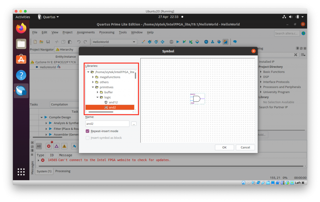
Click somewhere near the middle of the workspace in order to place a gate into the design.
You can click multiple times to place the component repeatedly, but we will only need one gate for this example.
Once done you can press the esc key to exit the symbol tool.
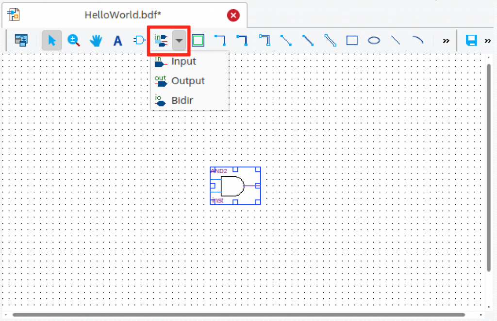
Adding pins
Next we will add some pins to the design. These will become the interface between the design and the physical IO pins on the chip. Later in the tutorial we will learn how to link these pins to the desired physical pins.
The pin tool consists of two parts, the main button and the arrow to the right-hand side. This arrow will drop down a small menu that allows us to choose the type of pin.
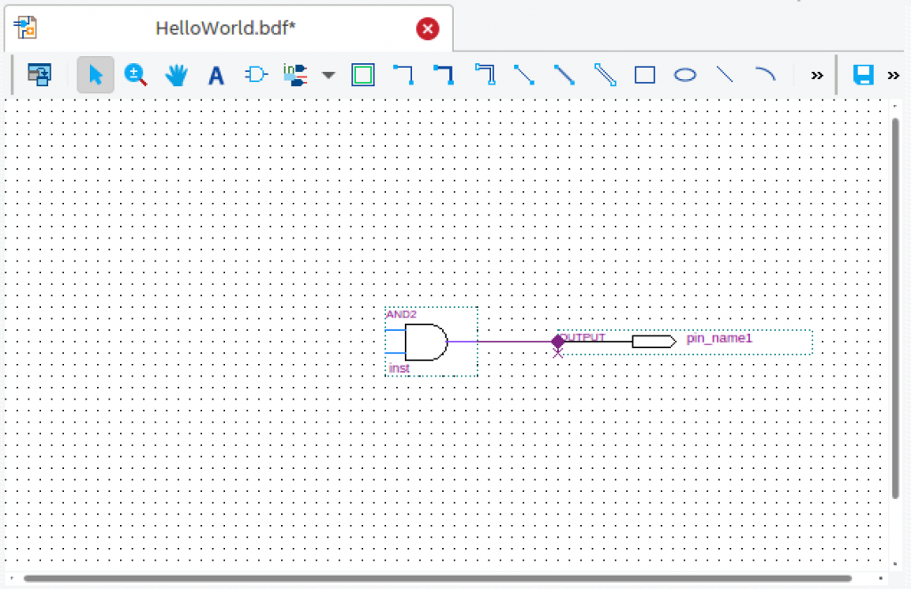
The type of pin is shown just above the pin placement icon. You can either click the main icon to place the current pin type that is selected, or click the arrow to place a specific pin. Go ahead and choose output.
Once we have placed the output pin, we need to connect it to the AND gate output pin. In order to do this simply click the end of either output and hold down the mouse button to draw a wire between the them.
Now let’s place two input pins and connect them to both inputs on the AND gate.
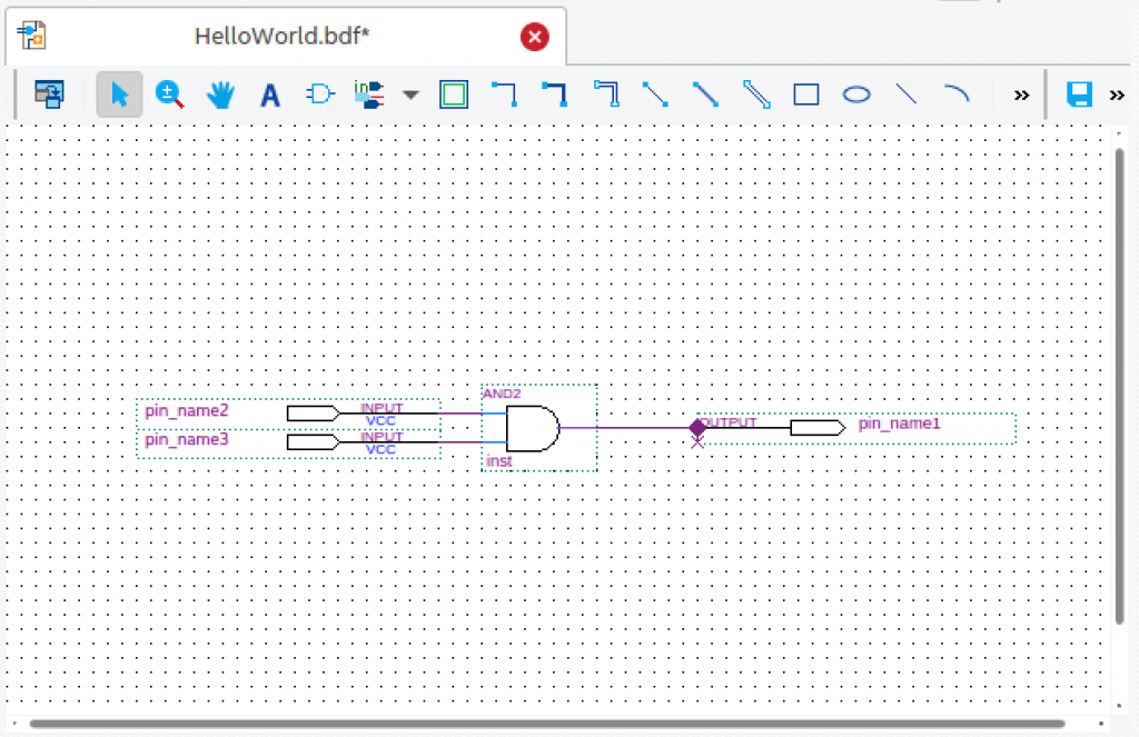
Lastly we will rename the pins to something more suitable. In order to change the name of the pin you can either double click the pin name in the editor or right click the pin and choose properties.
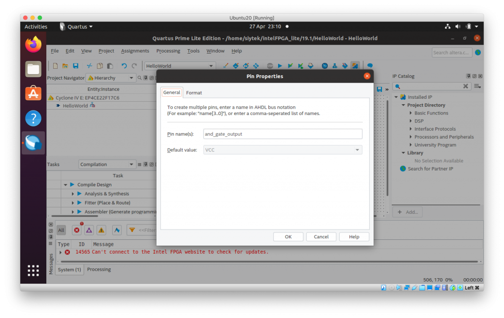
We will name the output and_gate_output and the inputs and_gate_input_a and and_gate_input_b. This will make it easier to identify the pins when we come to configure the hardware.
Configure the hardware
Now that we have finished our design, we are ready to compile it and load it onto our FPGA.
However we first need to decide which of the physical IO pins we wish to connect to our circuit.
For this simple example we will connect each input pin to a switch and the output pin to a LED.
We can then test the functionality of the AND gate by pushing the switches and observing the LED.
Physical connection
The physical connection will depend on the hardware you are using.
If you are building your own circuit, you can use any of the available IO pins. I will use the DE0-Nano as an example, but feel free to mimic the connections on a different board.
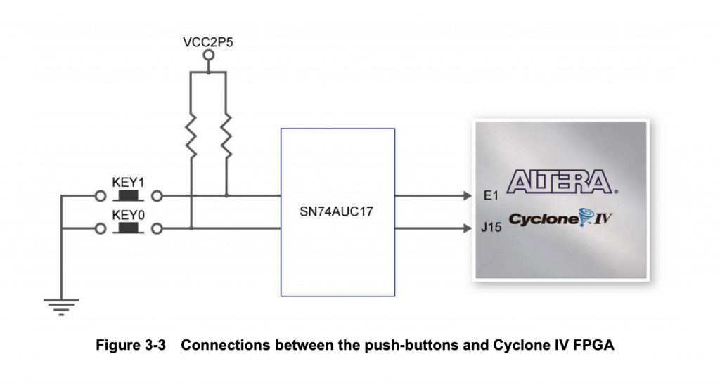
Switches
On the DE0-Nano the switches are connected to to pins E1 and J15. They are connected through a SN74AUC17 schmitt-trigger buffer and pulled high with pull-up resistors. The circuit should work ok without the buffer for test purposes.
LEDs
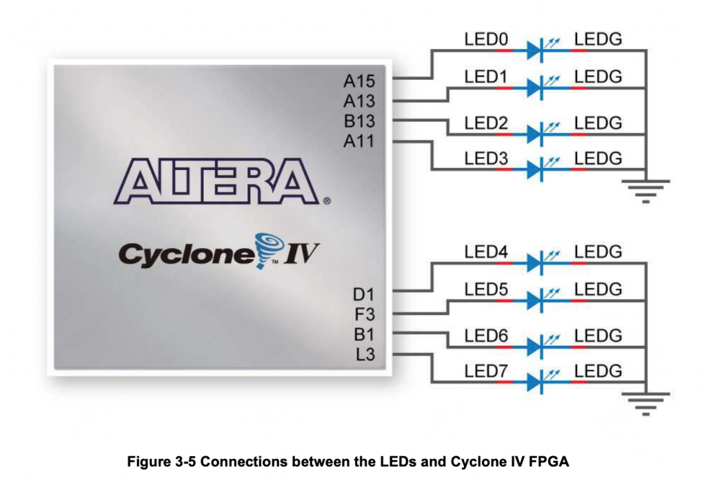
There are 8 LEDs on the DE0-Nano board and we can select any one of them for this project. For this project I will be using the LED connected to the pin A15.
For some reason the manual does not show any resistors in series with the LEDs, however I think this is an over-simplification and it is very unlikely that these LEDs are connected directly to the chip.
Therefore if you are building your own circuit, make sure that the LEDs are adequately current limited.
Pin planner
So now we should have three physical pins on the chip that we wish to connect to the output and two inputs which we included in our design. For the DE0-Nano we will be using the following:
- Pin E1 – a push button
- Pin J15 – a push button
- Pin A15 – a LED
In order to connect the pins in the design to the physical pins on the FPGA we are going to use a tool in Quartus called the pin planner.
This tool provides us with a map of available pins and functions and allows us to map parts of the design to the desired pins.
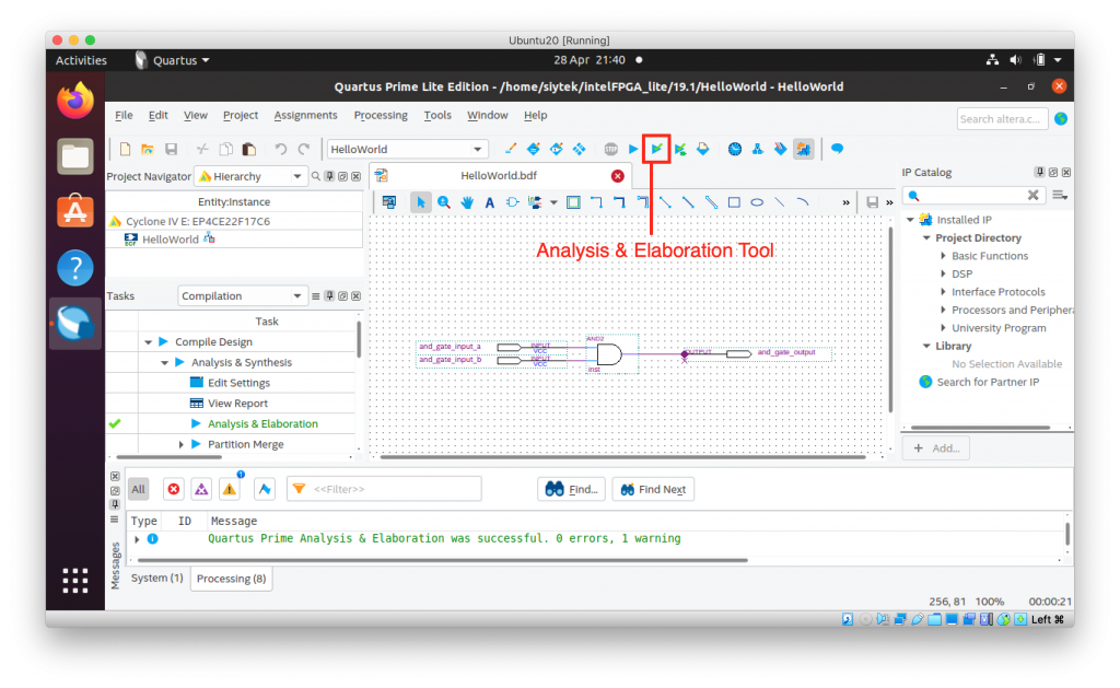
In order for Quartus to understand which parts of our design can be mapped, we first need to run a partial compilation on the design called analysis and elaboration.
Analysis and elaboration
There are different stages of processing required to convert our design into something that can be loaded on to the FPGA.
- Analysis – in this part of the process Quartus checks the design for any errors such as syntax or semantic error.
- Elaboration – in the first stage of compilation, Quartus maps out the design in RTL blocks. These are the building blocks within the FPGA that perform basic functions such as memory storage, logic gates and registers.
- Synthesis – in the final stage of compilation, Quartus synthesizes a design at the logic level, converting the RTL design into a gate level design.
In order to get our pins to appear in the pin planner we could run a full compilation. However this is not necessary as we only need to run the analysis and elaboration stage.
Quartus gives us three compilation tools that allow us to run different levels of compilation.
As the full compilation can take some time it makes sense to only run the necessary process. Go ahead and run analysis and elaboration using the tool found in the menu bar at the top of the screen.
Assigning the pins
Once the process has completed you will have a compilation report and the analysis and elaboration process in the left-hand menu will have a green tick next to it.
Now we can open the pin planner by clicking assignments > pin planner from the menu at the top of the screen.
The pin planner is a little complex at first glance, but it is fairly easy to use.
You will see a map of the FPGA with all of the physical pins and their functions.
We are interested in the list of pins at the bottom. If you have successfully completed the previous step you should see the pins listed. Go ahead and enter your switch and LED pins in the location box.
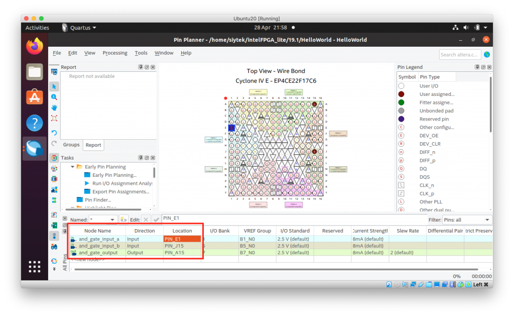
The input pins should correspond to the physical pins you have connected to the push buttons and the output pin should correspond to the output pin with the LED connected. Once you are done you can close the pin planner.
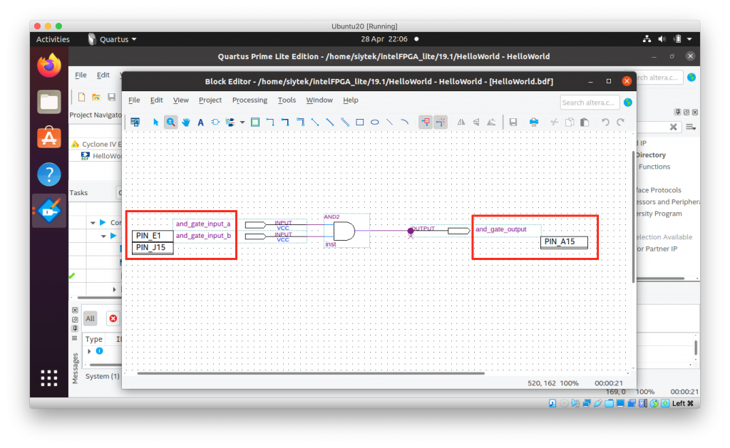
You should notice that Quartus has labelled the pins with the physical outputs that we have just assigned. Note that I have detached the design window to allow a larger work area.
You can detach a window by right clicking the tab at the top of the work area and selecting detach. You can also attach and detach windows from the window menu on the top menu bar.
Compile and program the FPGA
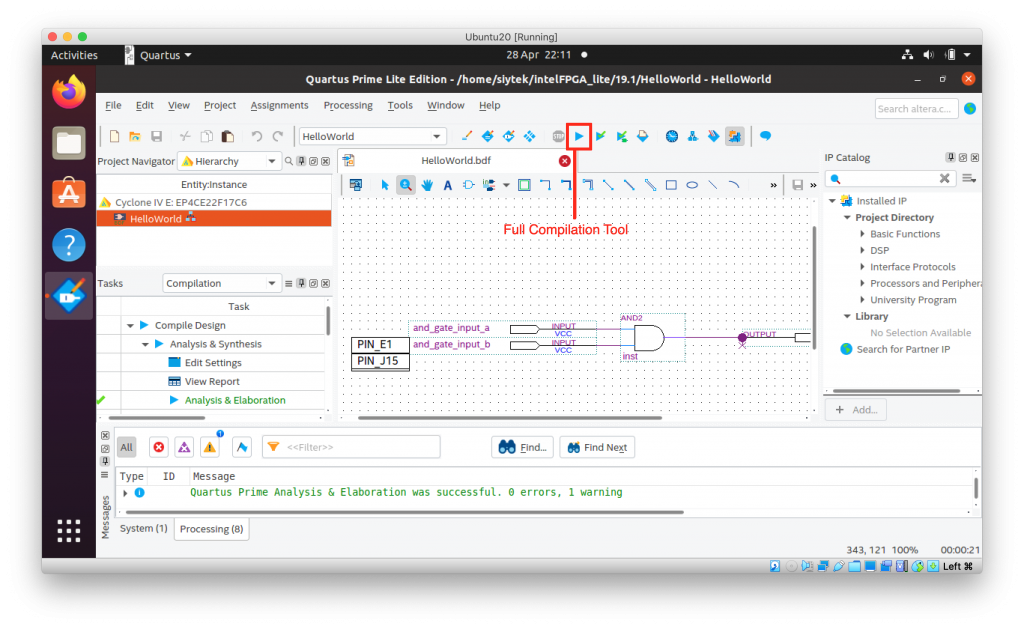
Now that we have our pins mapped we are finally ready to load the design on to the FPGA. Awesome!
Full compilation
In order to do this we must first run a complete compilation, which will synthesize the design and then create a binary .sof file that can be loaded on to the FPGA
Programming
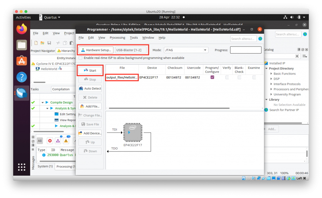
Once the compilation has complete we can open the programming tool in order to load our design on to the FPGA. You can either use the button on the top toolbar or click tools > programmer from the menu bar.
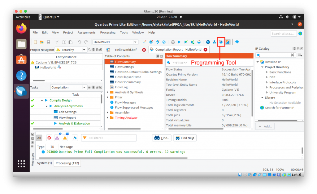
On the programming menu you should see your programmer (e.g. the USB-Blaster) appearing at the top of the screen if your device is connected and configured correctly.
If you see “no device” then you may need to select it by clicking hardware setup…
You should also see the .sof file appearing in the list. If not then go back and check that you performed the full compilation and encountered no errors.
Once you are ready, go ahead and click start to load the program on to the FPGA.
That’s it! You should now be able to illuminate the LED by pressing both of the switches at the same time. Next you can try swapping out the AND gate for some different logic in your design to see how the behaviour changes.
Conclusion
Personally I love developing on FPGA devices and I feel that they are often overlooked by the maker community in favor of standard microcontroller-based solutions like Raspberry Pi.
There are some complexities to overcome when first configuring the tools but once you have your “hello world” example up and running, it is easy to create some fun and rewarding projects!
Thanks so much for visiting my site! If this article helped you achieve your goal and you want to say thanks, you can now support my work by buying me a coffee. I promise I won't spend it on beer instead... 😏