
Looking to get started with Quartus quickly and easily?
Quartus can be a little daunting on first load due to the sheer number of tools, however once you overcome the basics it’s really quite easy to use.
This illustrated tutorial will teach you how to write and compile a simple Verilog program in a several easy steps.
At the end of the guide you will have a program up and running on your FPGA as Quartus won’t seem so complex!
- Prerequisite
- Create a new project
- Create a counter
- Create a clock divider
- Create a schematic
- Configure the hardware
- Program the device
- Conclusion
Prerequisite
You will of course need a computer with Quartus installed and running.
If you have not yet installed Quartus and/or are totally new to using it, I would recommend checking out my Quartus Prime hello world tutorial first to get you started.
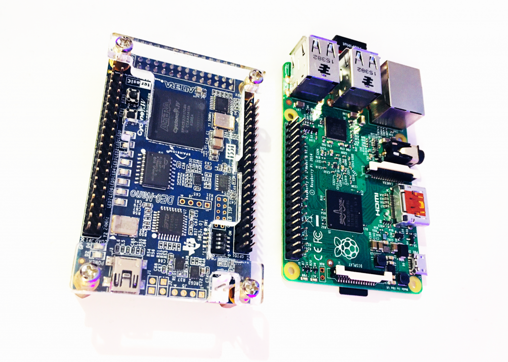
You will also need an FPGA to program! Personally I like using the Terasic DE0-Nano as it is slightly smaller than a Raspberry Pi and has many awesome features.
This means I can lazily sit back on my sofa and write code whilst having an awesome feature-rich FPGA board to hand.
We will be creating a simple binary counter that is driven from the FPGA external clock.
The counter will count upwards in binary and the result will be output to a series of LEDs.
If you have a DE0-Nano or similar then great! We will just use the onboard LEDs.
If you are using another board without LEDs then you can just connect some LEDs to the desired output pins using current limiting resistors.
I would recommend using a minimum of 3 LEDs in order to get a good view of the counting, however a total of 8 LEDs is prefered for full effect.
You can also modify the code easily if you wish to use more LEDs!
Create a new project
First we need to create a new project in Quartus, you can read up on how to do this in my Quartus hello world tutorial. Give your project a name, something like “counter” will do just fine.
No need to worry about adding files just yet nor selecting a simulator.
We just need to choose the correct chip. We will be learning how to add the following elements to the project.
- binarycounter.v | the binary counter Verilog file
- clock_divider.v | a component to divide the system clock
- counter.bdf | a schematic to link all of the elements
Create a counter
The primary element of the design will be the binary counter. It contains an 8-bit register that increments upwards each time the incoming clock signal rises from low to high.
Each bit in the counter register is output separately. We will connect these to a series of LEDs so that we can observe the value in the register. It also looks very cool!
Create a counter Verilog file
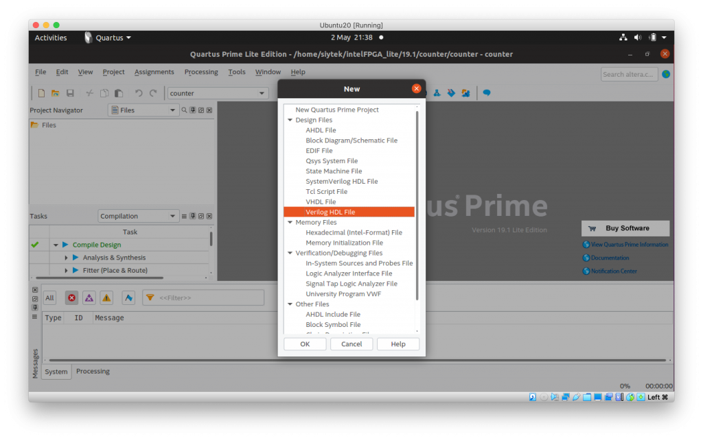
First we need to create a new Verilog file so that we can write the code that will create the device. Go ahead and click file > new and select verilog HDL file from the pop-up menu and click ok.
A new file will be created in the project workspace, go ahead and save it as something like binarycounter.v in the project directory. We are now ready to write the Verilog that will define the binary counter module in our project.
Define the module
The first line of code we need to write will define the module as well as the inputs and outputs. We will call this module bin_counter and we need to define the input and output clk and out respectively.
module bin_counter(clk, out);
We need to define clk as an input with the net type wire.
This represents a single wire entering the module that can store either a 1 or 0. We only need a single bit as the clock signal will either be high or low.
Next we need to define the output as a register, which is determined by the keyword reg.
This will create a register of the size specified in the [square brackets], in this case 8-bits (remember that 0 is counted as a bit).
module bin_counter(clk, out);

input wire clk;
output reg [0:7] out;
Create the module function
Now we can create the function of the module using the always statement.
Here we will specify the action that we wish to occur between the begin and end statement following the always statement.
We will also specify a condition in the sensitivity statement using the posedge statement.
This means that the action will only occur on the positive edge of the clk input, meaning when the clock transitions from a 0 to a 1.
We could also use negedge here too for when the clock transitions from a 1 to a 0, in this example it does not matter so much.
module bin_counter(clk, out);

input wire clk;
output reg [0:7] out;

always @ (posedge clk)
begin
	out <= out + 1;
end
Finally we can end the module using the endmodule statement. This completes our binary counter module so go ahead and save the file.
module bin_counter(clk, out);

input wire clk;
output reg [0:7] out;

always @ (posedge clk)
begin
	out <= out + 1;
end

endmodule
Create a clock divider
We are going to use the external clock connected to the FPGA in order to drive our counter. In order to increment the counter the clock signal must be connected to the clk pin that we created on the counter module.
However there is a problem! The speed of the clock connected to the FPGA super-fast! In the case of the DE0-Nano board it is 50MHz, meaning that the clock signal cycles from low to high and back again 50 million times per second!
This means that if we connect the clock directly to the counter, it will increment up 50 million times per second! If our LEDs are changing at this rate they will all appear as ‘on’ and we won’t see the counter working.
So what’s the solution? Quite simply we must slow the clock down by dividing it up. In order to do this we will create a clock divider which divides the clock by 50 million, creating an output clock signal with 1 cycle per second. Feeding this into our counter will increment it only once per second.
Create a clock divider Verilog file
In order to create a clock divider we will create a new module. Go ahead and create a new Verilog file called something like clock_divider.v and add it to the project.
Define the module
The first line of code we need to write will define the module as well as the inputs and outputs. We will call this module clock_divider and we need to define the input and output clk and out respectively.
module clock_divider (clk, out);
We need to define clk as an input with the net type wire. This represents a single wire entering the module that can store either a 1 or 0. We only need a single bit as the clock signal will either be high or low.
Next we need to define the output as a register with 26 bits. A register of this size will allow us to store a decimal value of 67,108,863. We will use the incoming clock to increment the register upwards by 1 and each time the maximum value is reached the register will return to 0.
If we divide the maximum value the register can hold by 50Mhz, we can calculate the time it takes for the register to elapse. In this case the most significant bit (MSB) in the register will transition from low to high and back again in 1.34 seconds.
Therefore if we take the MSB output from the register we will have a new clock signal with a cycle time of 1.34 seconds. Awesome!
module clock_divider (clk, out);

input wire clk;
output reg [0:25] out = 0;
Create the module function
We will of course need to increment our register just like we did in the previous counter module.
module clock_divider (clk, out);

input wire clk;
output reg [0:25] out = 0;

always @ (posedge clk)
begin
	out <= out + 1;
end
If we wanted to make the output clock cycle exactly one second long we could add 17,108,863 to the register value each time it elapses.
This would make the length of the count exactly 50,000,000 before the register elapses. However I wanted to keep this example as simple as possible.
Finally we can end the module using the endmodule statement. This completes our clock divider module so go ahead and save the file.
module clock_divider (clk, out);

input wire clk;
output reg [0:25] out = 0;

always @ (posedge clk)
begin
	out <= out + 1;
end

endmodule
Create a schematic
Now that we have created both of the modules we can tie it all together in a schematic and define the physical pins that we wish to use.
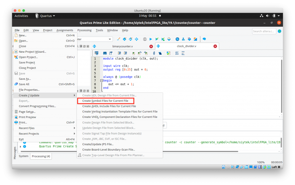
That first thing that we need to do is covert the Verilog files to symbols that will appear in the library so that we can place them into a schematic diagram. To do this make sure you have the Verilog file in focus in the project workspace, then click file > Create/Update > Create Symbol Files For Current File.
Once the compiler has completed building the symbol, switch to the other Verilog file and repeat the process. This will build a symbol for both the binary counter and clock divider modules.
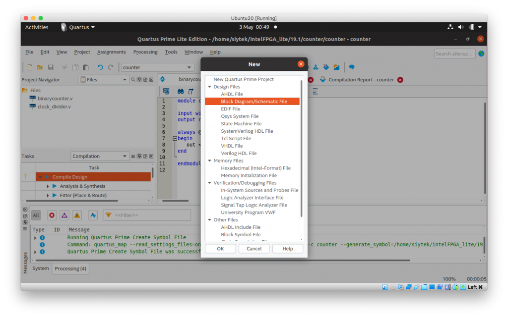
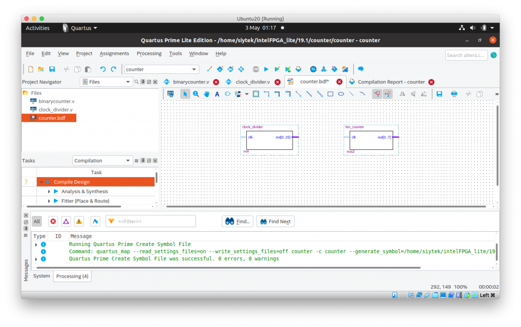
Next we need to create the main schematic file for our project. Go ahead and click file > new and then choose Block Diagram/Schematic File from the pop-up menu.
This will create a new schematic file in the workspace. Lets go ahead and save the file as counter.bdf.
Adding the modules
Now we can add the modules that we created earlier by clicking the symbol tool from the toolbar at the top of the workspace.
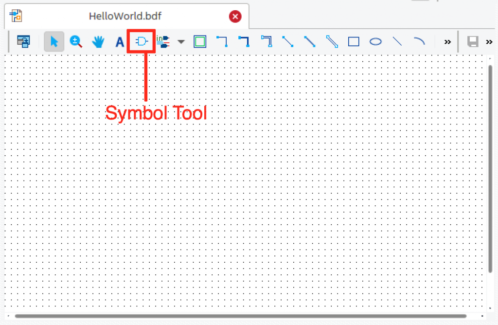
In the symbol explorer window you should see both modules that we created earlier located under the project folder.
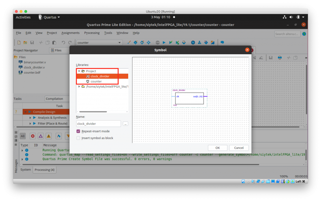
Go ahead an add a clock divider module to the left-hand side of the project workspace and a binary counter module to the right-hand side.
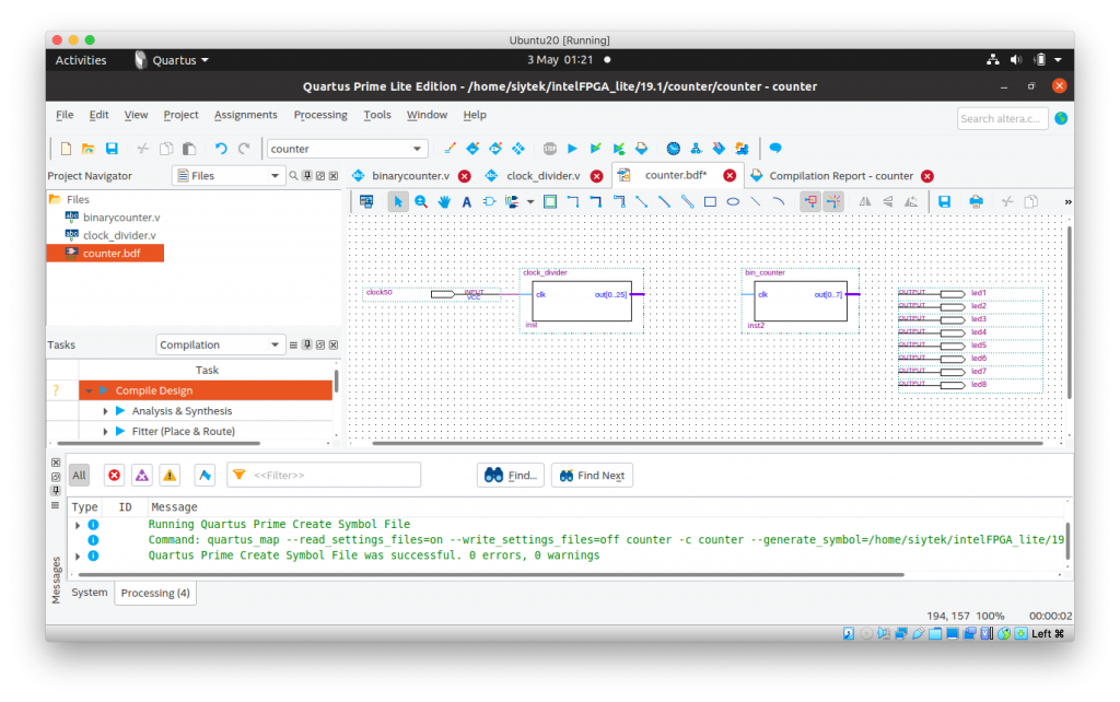
Creating the IO pins
Now that we have both modules located in our schematic, let’s add the IO pins. We need to add 1 input to the left-hand side for the clock and 8 output pins for each of the LEDs. We will name them clock50 and LEDn respectively.
We also need to connect the clock50 input pin to the clk input on our clock divider module.
Wiring the buses
You should notice that the outputs on both modules are represented by a thicker purple wire. This indicates that the connection is a bus containing more than a single bit. We must use either the bus or wire tool to draw new nets in the schematic.
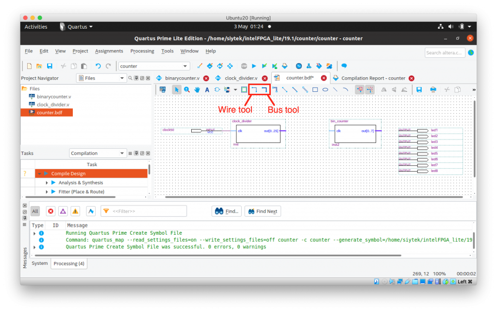
If we wish to break out a wire from a bus, we must utilise the naming convention. First we will extend the bus from the output of the binary counter down to the last LED output pin using the bus tool.
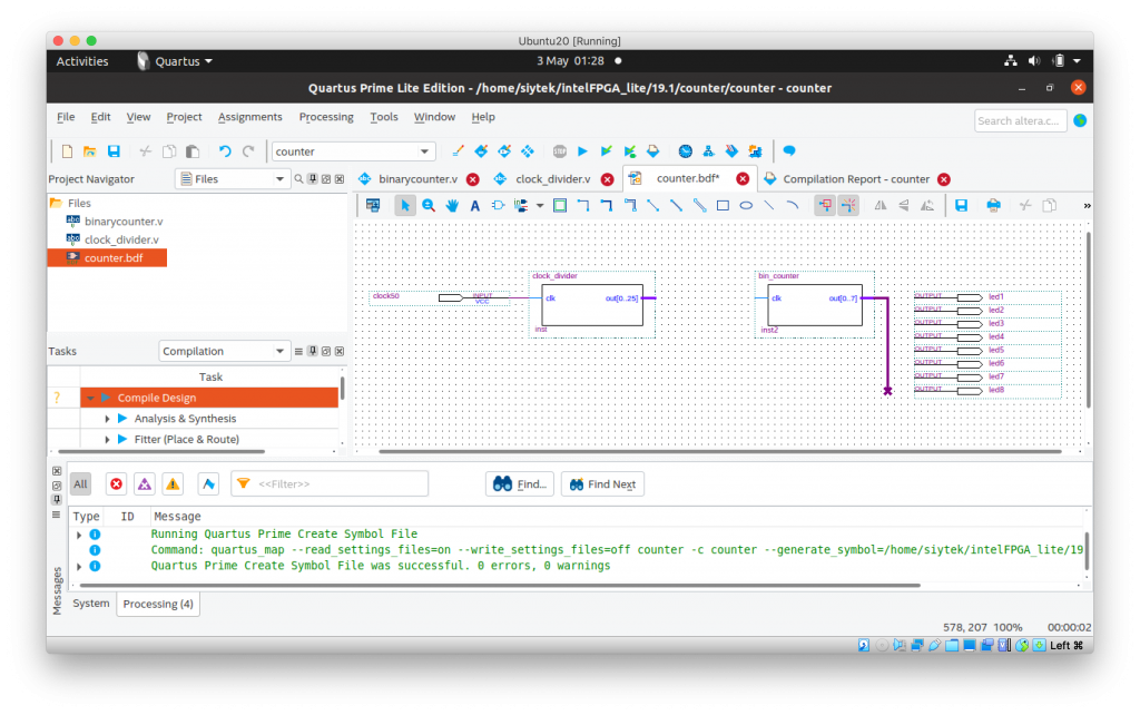
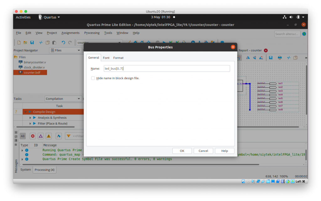
Now if we right-click the bus and then click properties we can give it the name led_bus. We will use [square brackets] at the end of the name to define how many bits we wish the bus to carry. These bits will numerically correlate to the binary counter output bits.
In order to break out a wire from the bus, we must first use the wire tool to create the wire from the bus to the location that we wish to connect it. Then we can name the wire using [square brackets] to specify the bit within the bus we wish to connect to.
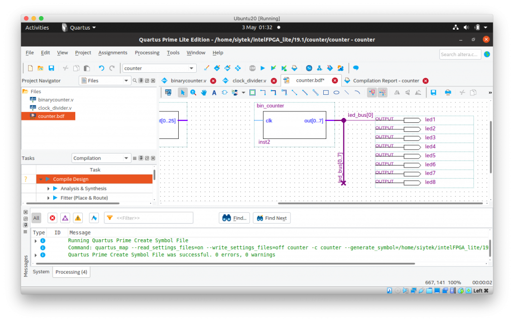
We can simply repeat this for all of the other LED pins, incrementally increasing the bit value within the square brackets.
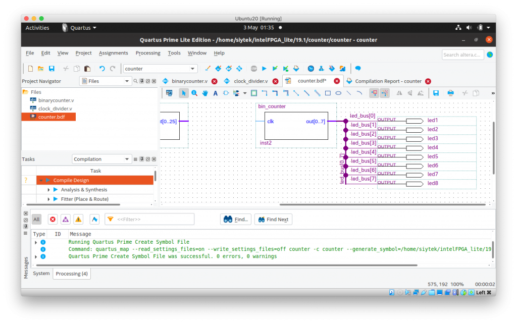
We also need to repeat this process with the output from the clock divider. Note that we only need to connect the MSB from the output to the binary counter clock input as this will generate the slowest signal, as we calculated earlier.
Therefore we will use the bus tool to create a short bus from the clock divider output, which we can then break out using the wire tool. We will link the bus to the clk input of the counter using a wire named clk[0] so that only the MSB is transfered.
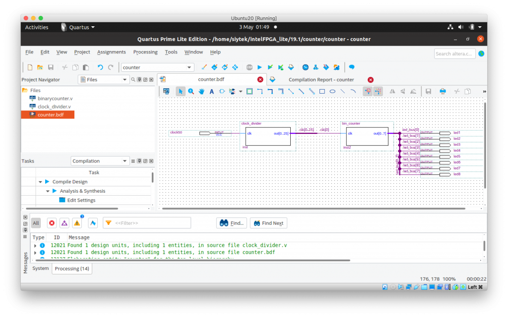
Configure the hardware
Now that our code and schematic are ready we can assign the physical pins on the chip to the IO in our design. If you are not familiar with how this is done I would recommend checking out the process in my hello world tutorial.
This process is also hardware dependent and for this tutorial I will be using the DE0-Nano board. If you are using different hardware you should ensure that you pick the pins that correspond to your device.
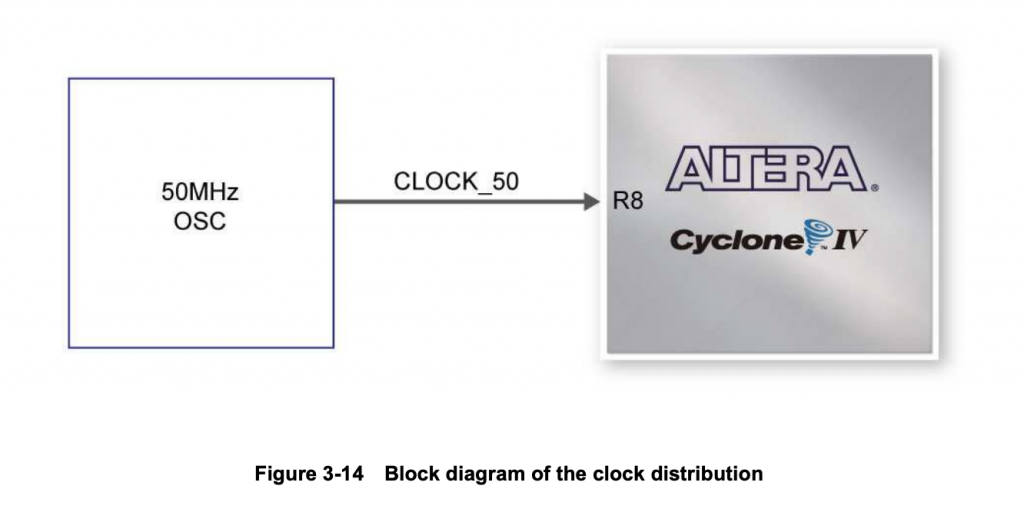
Clock input
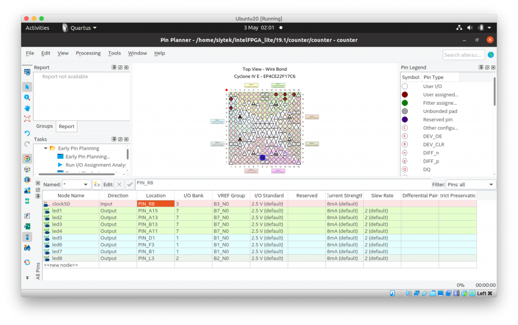
On the DE0-Nano the clock oscillator is connected to pin R8 as per the user manual. We need to assign the clock50 input pin to physical pin PIN_R8 in the pin planner.
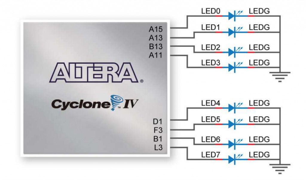
LED outputs
The onboard LEDs are connected to a series of pins as specified in the user manual. We should assign the pins top to bottom to the LED output pins 1 to 8 respectively.
Pin planner
You can access the pin planner by clicking Assignments > Pin Planner from the menu bar at the top of the screen. Don’t forget to run the analysis & elaborate process first, otherwise your pins will not show in the planner.
Go ahead and assign all of the inputs and outputs in the pin planner. If you are using the DE0-Nano, you can use the following list for reference.
- clock50 | PIN_R8
- led1| PIN_A15
- led2| PIN_A13
- led3| PIN_B13
- led4| PIN_A11
- led5| PIN_D1
- led6| PIN_F3
- led7| PIN_B1
- led8| PIN_L3
Program the device
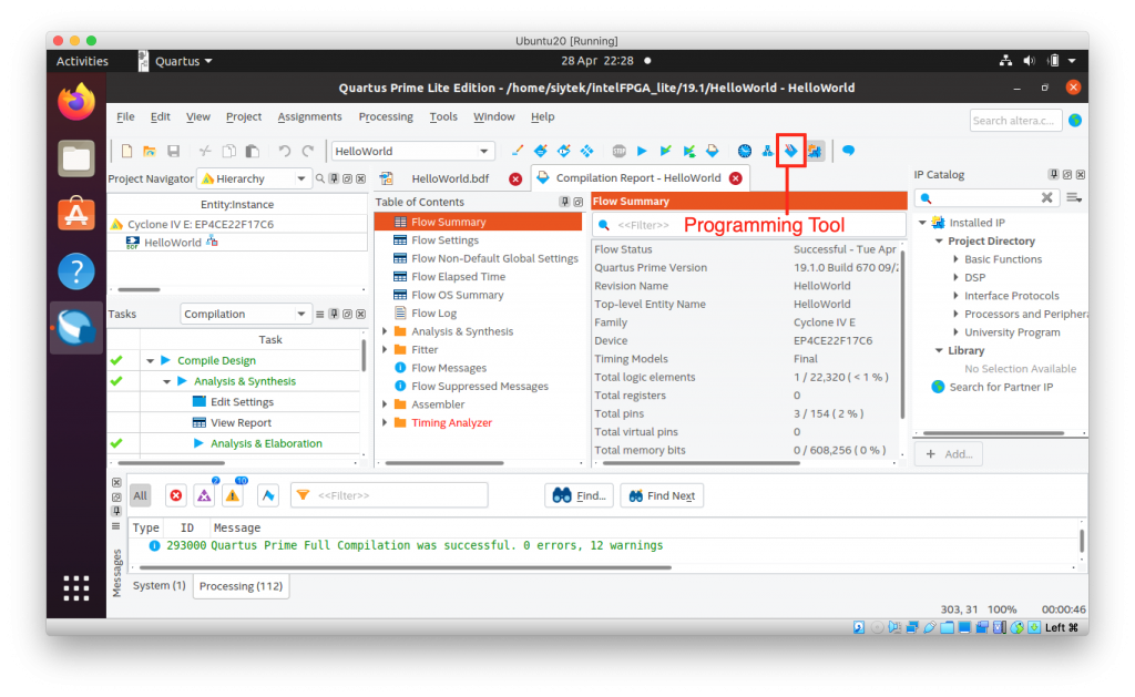
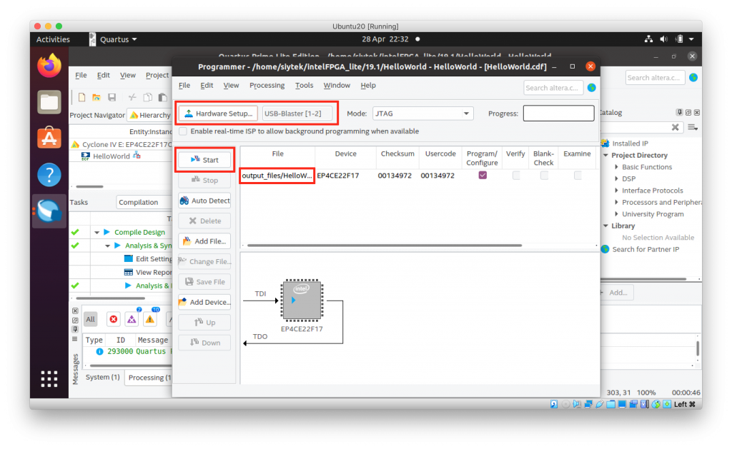
Once you have finished mapping the pins, go ahead and run a full compilation on the project. This will prepare the necessary files for programming.
Once the compilation has complete we can open the programming tool in order to load our design on to the FPGA. You can either use the button on the top toolbar or click tools > programmer from the menu bar.
Conclusion
With our design flashed to the chip we should now see the contents of the counter register displayed on the LEDs. Awesome!
There are many stages required to perform this simple demonstration, however Quartus is an immensely powerful tool and from here it is easy to build some far more powerful applications!
Don’t forget to check out some of my other FPGA related tutorials or check out all of my general rambling about electronics right here!
Thanks so much for visiting my site! If this article helped you achieve your goal and you want to say thanks, you can now support my work by buying me a coffee. I promise I won't spend it on beer instead... 😏


I tried it on cyclone II but it didn’t work on the hardware. I changed the pin assignments accordingly.
Thanks for visiting Sayali, yes you would need to select the pins according to the hardware. Did you get everything up and running ok?
The software used is 2009 Quartus II and device is FPGA starter kit seated with EP2C20F484 (Cyclone II). The problem is if we assign the pins mounted on the board all is well( PB-SW-LED). If the I/O pins are assign to GPIO external com port the system is not working.
Running simple test as: External switch — internal LED: simple circuit
VC3.3V _____/ ________GPIO plug to internal LED on switch close the LED should be ON nothing happens if the circuit assigned internally all works OK; meaning switch and LED internal on test kit.
So I checked with on board switches and LED and it worked alright. But when I tried using GPIO (external pins) it didn’t work. What am I doing wrong?