If you are looking to get your PCB fabricated or just want to learn how to output Gerber and Excellon manufacturing data, you have come to the right place!
After working in various PCB engineering and management job roles for the last decade I have learned a thing or two about PCB manufacturing. However it can be said I am still somewhat of a newcomer, even with a little over 10 years experience.
A PCB File Format History Lesson
The real gurus of this industry who have been around for 20+ years never fail to teach some fascinating history lesson when seeking technical advice. The reason we do things the way we do them in the industry is almost always for historical reasons.
What is a Gerber File, anyway?
Gerber is the name of a file format used in printed circuit manufacturing. It is the industry standard file format used to transfer data between designers and PCB fabricators.
The file format was originally developed by Ucamco, a company who develops leading solutions for PCB manufacturing facilities.
The best description of the Gerber file format can be found at the source, I thought there was no need to rewrite it:
The Gerber file format is the de facto standard for printed circuit board (PCB) design data transfer, called the backbone of the electronics fabrication industry. All PCB design systems output Gerber files and all PCB fabrication software can handle them, enabling PCB professionals to exchange PCB design data securely and efficiently.
Gerber layer files represent copper layers, solder mask, legend, and drill and route data. Attributes provide meta-information about these images, such as whether a graphics object is an SMD pad, a via pad or a fiducial, or net names of connections. The Gerber job file transfers PCB fabrication characteristics, such as thickness or finish, in a standardized and machine readable manner. The Gerber format is simple, compact and unequivocal. Thanks to its use of printable 7-bit ASCII characters, it is portable, human-readable and easy to debug. Implementations are thoroughly field-tested and debugged.
https://www.ucamco.com/en/gerber
Gerber files consist of a table of apertures that can be used to create features such as lines and other shapes. This is a throwback to when plotters were used to produce artworks that would be used in the manufacturing of PCBs.
Older plotters actually had these physical apertures accessible within a wheel and the machine could select a particular aperture in order to draw the artwork as it appeared in the Gerber data.
This was done by shining a UV light through the aperture in order to expose the artwork in a process similar to film photography.
Nowadays far more sophisticated systems are used, such as UV laser or LED imaging systems that can expose film photoresist or solder masks without the need for artwork.
However the Gerber data format has remained industry standard for representing the various PCB layers during manufacturing. However we now have specialist CAM software suites that interpret the data and are able to output it in a multitude of formats for various machines.
What is Excellon Data?
Excellon data is also a file type used in PCB manufacturing. Like Gerber it exists due to historical reasons, however it is specifically used for PCB drilling.
Originally the manufacturers of drilling and routing NC (numerically controlled) machines used their own proprietary data formats similar to G-Code.
Each variant of machine programming code was generally named after the machine manufacturers themselves. The Excellon drill data format is derived from the company Excellon, who make NC drilling machines for PCB.
Excellon data became one of the more popular choices for drill data, with many fabricators preferring this file type. It is therefore recommended to use it when supplying drill data to the board fabricator.
How To Output PCB Manufacturing Data From KiCad
In order to turn your on-screen design into a real world printed circuit board it is necessary to output all of the necessary data.
Output Gerber data
We will use the two aforementioned file formats, Gerber and Excellon. The latter will be used for drill data and the former for all other layers.
Step 1: Open the project in the PCB board editor that you wish to use for outputting data.
Step 2: Click File > Fabrication Outputs > Gerbers (.gbr) to open the plot file exporter.
Step 3: The default parameters will give you a very good starting point and it may not be necessary to alter them.
Plot Format: Should be left as Gerber unless you wish to plot in a different format. Here you can also choose PDF should you wish to create a PDF diagram instead of Gerber manufacturing data. Other plot formats such as .svg are also available here should you require them.
Include Layers: The default options will likely give you all necessary layers, amend as necessary.
General Options: These can be set as per your own personal preferences. Unless you wish to change anything, the default options will be good for board fabrication.
Gerber Options: These can be left as default for board fabrication purposes.
Output Directory: Choose the location for the outputted files.
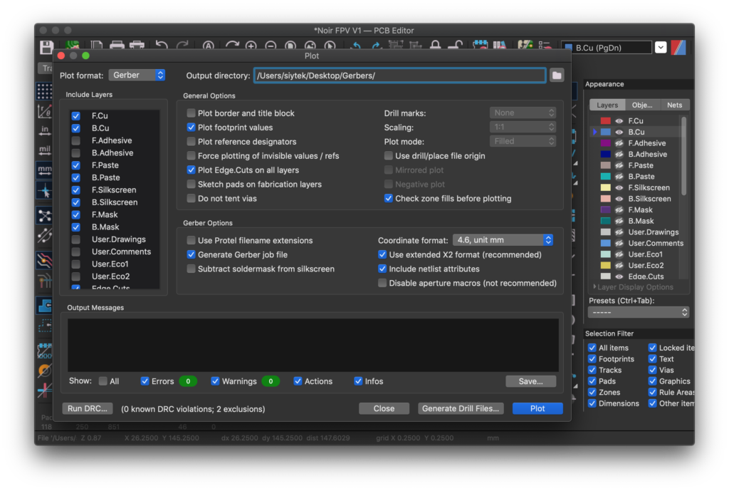
Step 4: Once you are happy with the settings and file path, click plot to output the files.
Output Drill Data
Step 5: In order to output the drill files, you can click the Generate Drill Files button from the plot file exporter window to open the drill file exporter. It is also accessible from File > Fabrication Outputs > Drill Files (.drl)
Step 6: The default parameters will give you a very good starting point and it may not be necessary to alter them.
Drill File Format: The default settings here will be good for fabrication in mostly all cases. Some fabricators may prefer the PTH and NPTH (plated and non-plated through holes) to be supplied in the same or different files but it shouldn’t matter too much.
Map File Format: This is the format that the drill drawing will be output in. Gerber may be the best option here, although PDF would also be a good choice. Fabricators will be able to work with either of these options.
Drill Units: This should be to your preference, but it can help to tell the fabricator what units are being used.
Zeros Format: In the modern day and age there is no need to suppress the zeros in order to compress the file size. This option would be best left as decimal. If the fabricator has trouble with the file, opt for the keep zeros option instead.
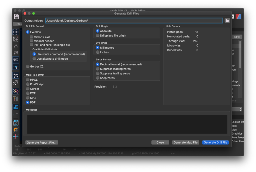
Step 7: Once you have chosen the desired output parameters, click Generate Drill File in order to output the .drl drill data and then click Generate Map File in order to output the drill drawing.
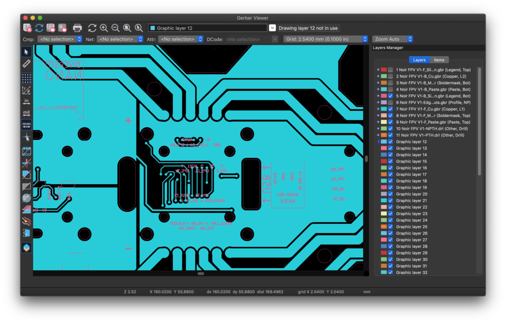
Checking the Data
Once you have output all of the files it can be a good idea to check the data. KiCad has a superb Gerber viewer that can be used to check the outputted data.
Open the Gerber viewer from KiCad main project window and load in the files outputted in the preview step.
File > Open Gerber Plot File(s) to load in the Gerber data (.gbr files).
File > Open Excellon Drill File(s) to load in the drill data (.drl files).
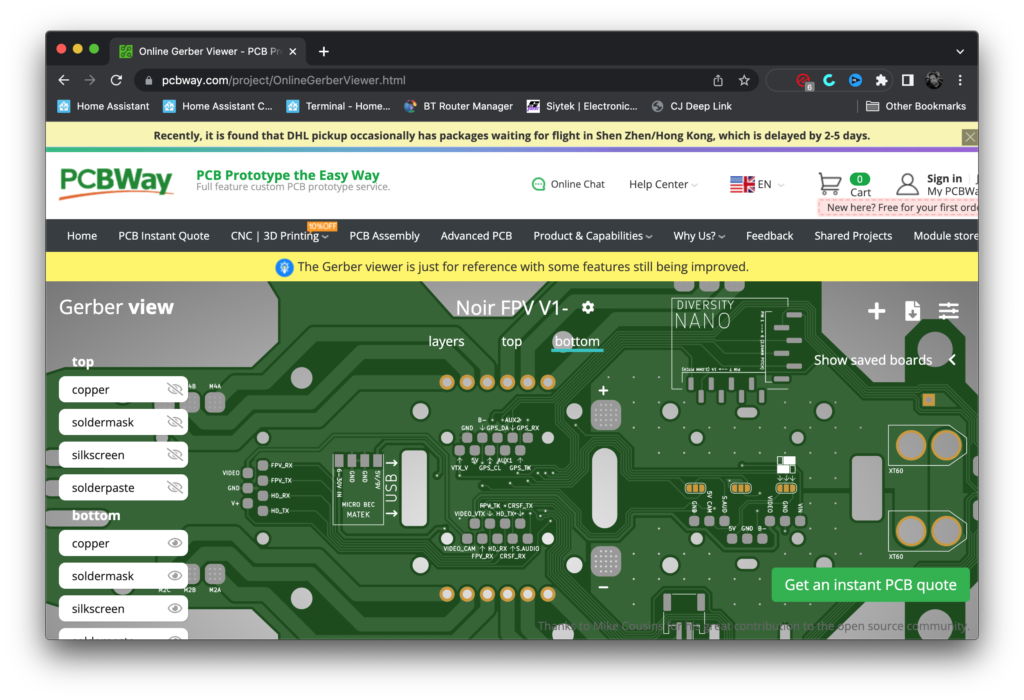
It is also possible to check the Gerber data with an online Gerber file viewer. Some fabricators such as PCBWay now offer Gerber viewing at the quotation state, which can be very useful!
You can try the PCBWay online Gerber viewer here: https://www.pcbway.com/project/OnlineGerberViewer.html
Here it is possible to really visualise what the PCB will look like once it has been fabricated!
Conclusion
With a little bit of knowledge about the history of printed circuit manufacturing, it is not so difficult to understand some of the industry standard file types used in PCB fabrication.
As we have seen in this tutorial, KiCad makes it very easy to output data in the correct format for PCB fabrication and although Gerber can now be considered a very old file type, it can certainly be said that it remains the king of the PCB industry!
I hope this tutorial has helped you output the data that you needed to realise your own PCB designs! Why not check out my KiCad frequently asked questions for some further reading!
Thanks so much for visiting my site! If this article helped you achieve your goal and you want to say thanks, you can now support my work by buying me a coffee. I promise I won't spend it on beer instead... 😏