
If you are like me, a KiCad noob, and you recently decided to embark upon a journey to learn KiCad, you may very well benefit from checking out these top questions asked by KiCad beginners.
Whether you are a seasoned PCB designer migrating from another software (such as EAGLE) or you are completely new to PCB design, these answers to frequently asked questions are sure to be of assistance.
After all I should know… just lately I was asking the same questions myself!
The following mini-guides are all for the latest version of KiCad 6 at the time of writing.
- How do I add a resistor in KiCad?
- How do I add a custom library to KiCad?
- How do I add a footprint to a library in KiCad?
- How do I add a mounting hole in KiCad?
- How do I add a ground plane to a board in KiCad?
How do I add a resistor in KiCad?
In order to add a resistor in KiCad, first it must be added to the schematic design and then connected as necessary.
Once the symbol is placed within the schematic and connected, it will migrate to the board once it has been created.
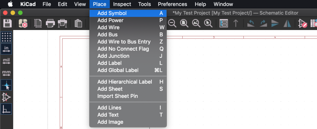
Step 1: In the schematic editor, click Place > Add Symbol. You can also simply press ‘A’ on the keyboard for a shortcut.
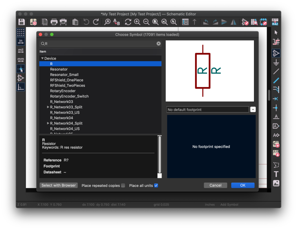
Step 2: The Choose Symbol dialog box will open. Enter ‘R’ into the search box at the top and select ‘R’ under device. Click OK to place the resistor into the schematic.
Step 3: Click to place the resistor into the schematic. Using the wire tool, connect the resistor as per the requirements of the design. Or for testing purposes, just leave it disconnected for now!
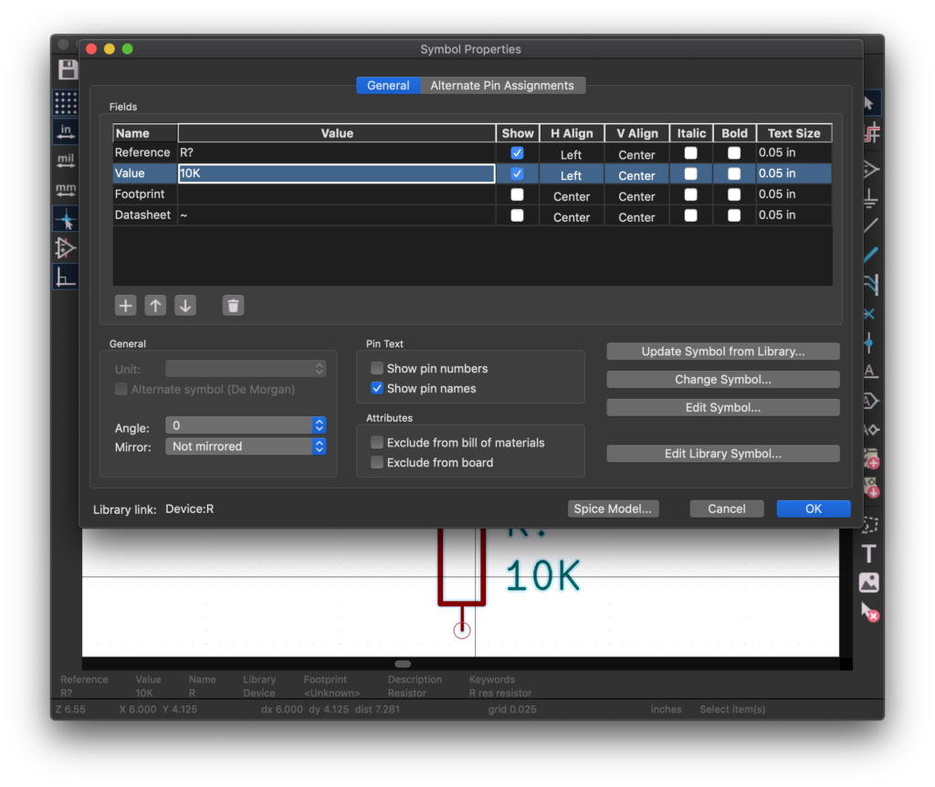
Step 4: Double-click the resistor symbol in the schematic sheet to change relevant properties. Most likely you will want to add a value, such as 10K as in this example.
Step 5: Click Tools > Annotate Schematic and then click OK. This will add a reference designator to each component. In the case of this example, a sole ‘R1’ designator will be given to the single resistor within the schematic.
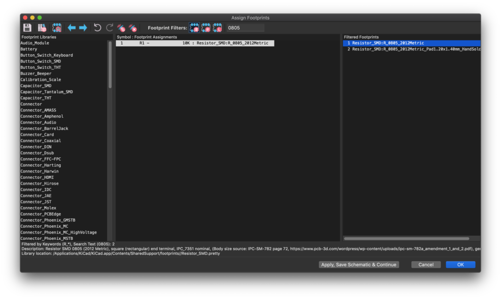
Step 6: Click Tools > Assign Footprints in order to open the Assign Footprints tool. In the case of our example, we see one sole resistor, R1.
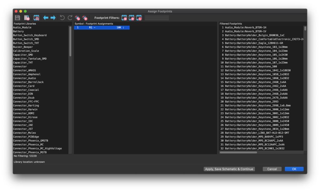
Step 7: Using the Footprint Filters, locate the correct footprint. In this case we have selected a standard 0805 footprint. Click OK once the footprints have been assigned.
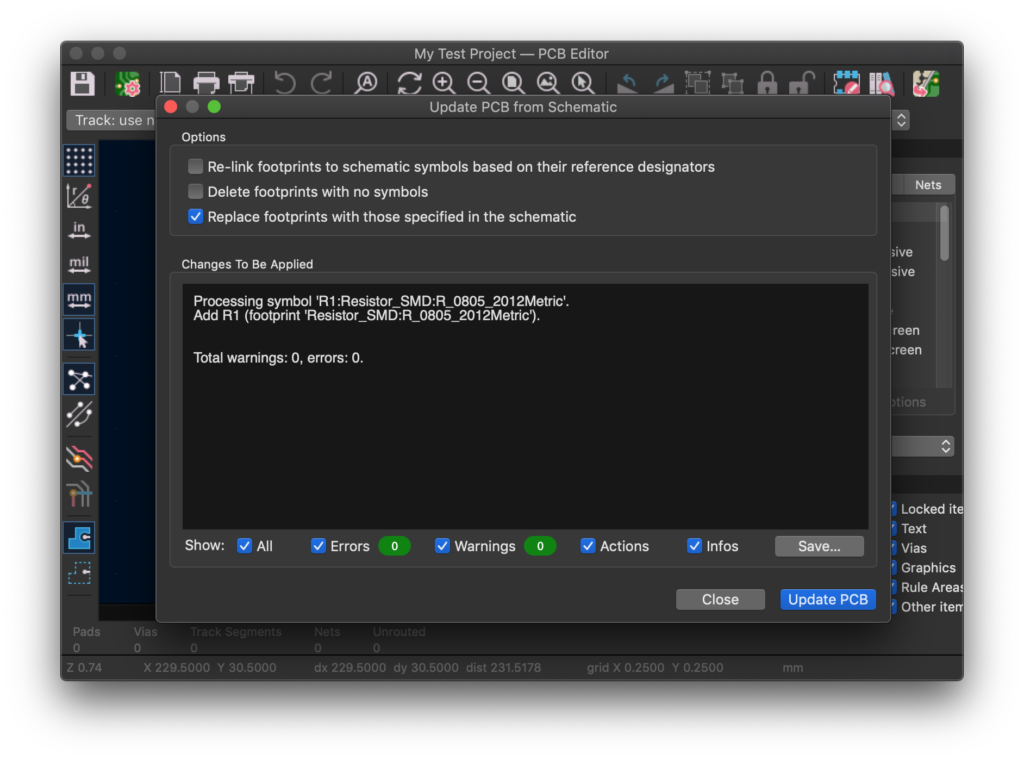
Step 8: Back in the schematic editor, click Tools > Update PCB From Schematic. Confirm that there are no errors and click Update PCB then click close.
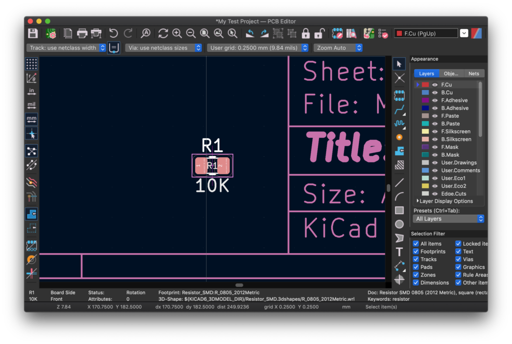
Step 9: Click to drop the components from the schematic, ready to be placed and routed. In the case of our example, just the one resistor.
Step 10: We are done! Time to make a cup of coffee…
How do I add a custom library to KiCad?
After some time it is inevitable that you will encounter the situation whereby a component that you require is not located within the KiCad default libraries.
You have two choices, either you can create a new footprint or you can add a custom third library to KiCad, which contains the component and/or additional components.
For the purpose of this mini-guide, let’s add the Digi-Key library to KiCad, although you can add any library that you prefer.
Step 1: Download the Digi-Key KiCad Library and unzip it into your chosen directory.
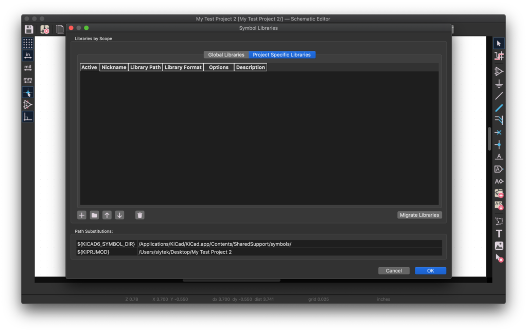
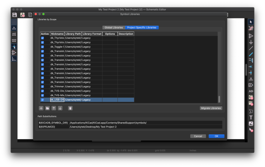
Step 2: Open the schematic editor and click Preferences > Manage Symbol Libraries…
Step 3: Choose from the tabs global libraries or project specific libraries depending on whether you would like the library to be accessible by all projects or only the current working project. In this case we will add only to the project.
Step 4: Click the folder icon (next to the + icon) and navigate to the symbols directory /digikey-symbols within the files unzipped earlier, or any directory containing the symbols you wish to add.
Select all of the .lib files and click OK to add them. This will populate the dialog box with all of the new symbols. Click OK to finish adding.
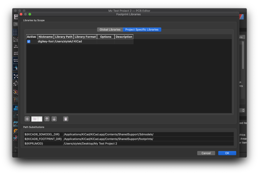
Step 5: Open the PCB board editor and click Preferences > Manage Footprint Libraries…
Step 6: Choose from the tabs global libraries or project specific libraries depending on whether you would like the library to be accessible by all projects or only the current working project. In this case we will add only to the project.
Step 7: Click the folder icon (next to the + icon) and select the footprints directory /digikey-footprints.pretty within the files unzipped earlier, or any directory containing the footprints you wish to add.
Note that this is slightly different to adding symbols, you should select the whole folder and add.
Step 8: Click OK to complete and that’s it! You will now find the footprints and symbols from the third party library in your project!
How do I add a footprint to a library in KiCad?
If you are unable to find a third party library containing the correct footprint it is likely that you will need to add your own. In this case it is possible to add a footprint to a library in KiCad.
Step 1: Open the footprint editor. If you wish to add a footprint to an existing library, locate it in the left-hand tree. If not then you can create a new library by clicking File > New Library…
Step 2: For this example we can create a new library Test Lib. Right-click the library and choose New Footprint. A dialog box will open, choose your desired name and select the footprint type.
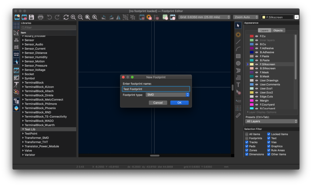
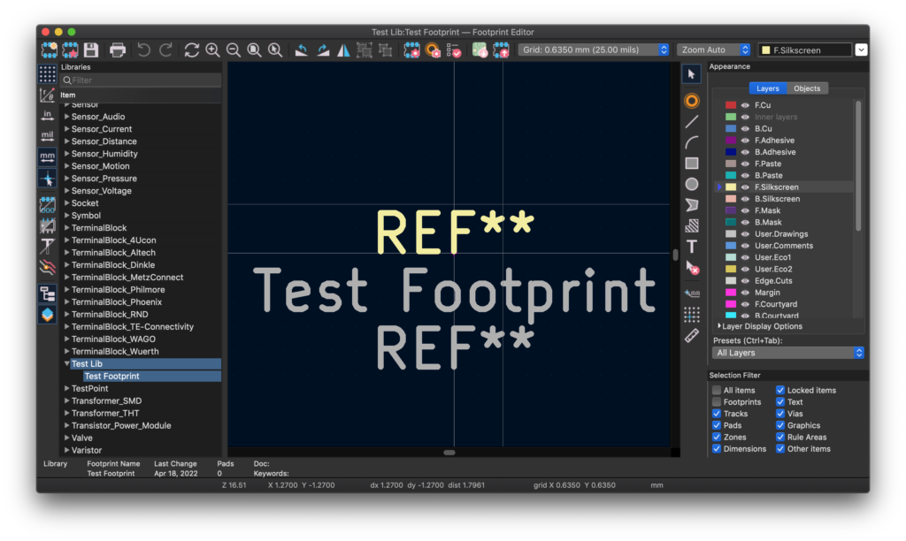
Step 3: Click OK and you are done! A blank footprint will open, where you can create a new footprint design.
How do I add a mounting hole in KiCad?
Mounting holes, or NPTH (non-plated through holes), which would usually be used to fix a PCB within some kind of enclosure are a little tricky to find.
There is no specific tool for adding them (like you might find in other programs, such as EAGLE), but instead they can be found as an actual library component.
Step 1: Open the PCB board editor and click Place > Add Footprint (or simply press the ‘A’ key).
Step 2: In the add footprint dialog box, search for mountinghole and choose your desired size from the list.
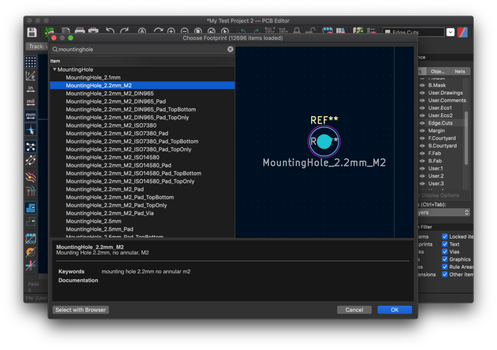
Step 3: Click OK to add the mounting hole to the board layout. Rinse and repeat for all desired mounting holes!
How do I add a ground plane to a board in KiCad?
Adding a ground plane in KiCad is very straight forward, I really like the way they implemented the ground plane tool.
Step 1: Set the working layer as the copper layer you wish to add the plane to. This can be done by double-clicking the layer in the right-hand toolbar, so that the blue triangle appears next to it.
Step 2: Click Place > Add A Filled Zone or choose the tool from the right-hand toolbar. Click the point where you wish to begin drawing the plane. A properties dialog box will open.
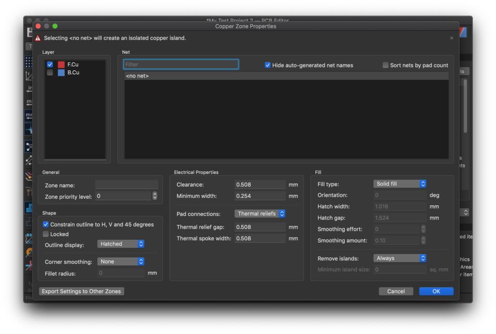
Step 3: Select the required options. As a minimum the copper layer and net should be chosen. Choosing <no net> will create a copper pour that is not connected. Click OK to begin drawing the ground plane.
Step 4: Draw the ground plane in the desired area. A single left-click will add a node, a double left-click will complete the polygon.
Step 5: Click Edit > Fill All Zones, or simply press the ‘B’ shortcut key to fill the ground plane in order to complete the process.
Conclusion
When first delving into the world of KiCad it can be a little intimidating, with so many new things to learn. However a little perseverance can lead to some very rewarding results!
I hope these popular frequently asked questions have somewhat helped you along your journey of learning KiCad and I would invite you to do some further reading!
Thanks so much for visiting my site! If this article helped you achieve your goal and you want to say thanks, you can now support my work by buying me a coffee. I promise I won't spend it on beer instead... 😏