
You probably already know that is important to tell KiCad the capabilities and limitations of your chosen fabricator to ensure the factory can manufacture your board. But how do we do this?
This tutorial will teach you how to set up design for manufacture (DFM) in KiCad 6.
If you are new or unfamiliar with KiCad 6 you may want to check out this tutorial first.
If you have never used KiCad or you are using an older version, go ahead and download the latest version of KiCad 6 before you begin.
What is DFM for PCB?
There are many process steps involved in PCB manufacturing. I spent 10 years working in various PCB manufacturing roles and I can tell you that the list of process steps is considerably longer than you can imagine!
Each step in the manufacturing process requires certain machinery and depending on the machines uses, there are certain tolerances that can be achieved.
For example a hole can be drilled in a PCB, typically down to 0.2mm in diameter without much difficulty. The position of the hole drilled will have a tolerance of 0.1mm relative to the position within the data.
This is an example of a capability and a tolerance, limitations imposed by the machinery used for drilling the holes. Each process step has such capabilities and tolerance.
Therefore when designing a PCB it is important not to exceed these capabilities, otherwise there will be problems during manufacturing.
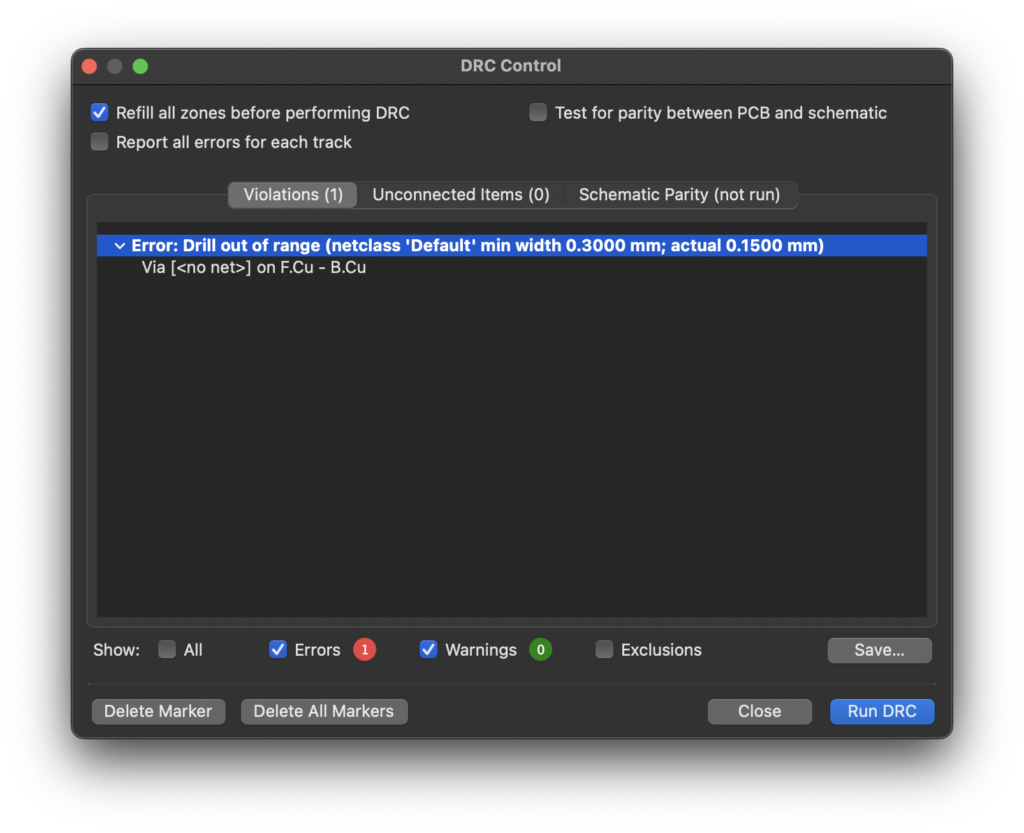
For example if you design a board that has 0.1mm diameter holes, but the smallest holes the board fabricator can drill are 0.2mm, it will not be possible to manufacture your board!
The solution to this is to enter a set of design rules into KiCad. These rules tell KiCad what the minimum and maximum capabilities are based upon information from the board fabricator.
For example if we tell KiCad the minimum hole diameter is 0.3mm but we accidently use a 0.1mm drill in our design, KiCad will flag a problem during a design for manufacture (DFM) check and ask us if we are sure we wish to use a hole size below the minimum.
Where Do We Find DFM Values To Use In KiCad?
So now that we understand the importance of a DFM and why we need to tell KiCad these values, where do we get such values?
These values are determined directly by the capability of the manufacturer. Therefore each manufacturer can have different values and we must find the values at the manufacturer.
It is common for a PCB fabricator to provide capability information on their website. Let’s take a look at the DFM values from three popular choices:
You can click the link to look at the individual capabilities for each fabricator, however let’s take a look at a comparison summary of some of the more notable points.
| PCBWay | JLC PCB | Seeed Studio | |
| Number Of Layers | 1 – 10 | 1 – 6 | 1 – 6 |
| Maximum PCB Dimension | 500 x 1100 mm | 400 x 500 mm | 500 x 500 mm |
| Board Size Tolerance | ±0.2mm | ±0.2mm | ±0.2mm |
| Board Thickness | 0.2 – 2.4mm ±10% | 0.4 – 2mm ±10% (>1.0mm) ±0.1mm (<1.0mm) | 0.6 – 3.0mm ±10% (>1.0mm) ±0.1mm (<1.0mm) |
| Minimum Track | 0.1mm | 0.127mm (1-2 layers) 0.09mm (4-6 layers) | 0.1mm |
| Minimum Spacing | 0.1mm | 0.127mm (1-2 layers) 0.09mm (4-6 layers) | 0.1mm |
| Minimum Hole Size | 0.2mm ±0.08mm | 0.2mm +0.13/-0.08mm | 0.2mm ±0.05mm |
| Minimum Annular Ring | 0.15mm | 0.13mm | 0.1mm |
| Minimum Legend Width | 0.15mm | 0.15mm | 0.1mm |
These are just some of the design for manufacturing parameters in order to give an example. As you can see they are all quite similar across three manufacturers.
It is worth mentioning that a good board fabricator will check the design during the CAM engineering stage, prior to manufacturing.
If there are aspects of your design that cannot be manufactured, the fabricator should inform you and propose a solution to fix the problem before manufacturing begins.
The fabricator may not provide values on their DFM/capabilities page for absolutely every parameter, but you should enter as much information as possible to minimise the chance of having any problems.
You should complete as much of the DFM as possible in order to streamline the process but you do not need to worry if there are a few details missing.
It is also worth noting that just because a PCB manufacturer has a certain capability does not mean that you should use it.
For example do not use 0.2mm vias if you have room to use 0.4mm vias. Even if the manufacturer can drill 0.2mm holes it is still easier and will produce better yields using the larger 0.4mm size.
How To Use DFM Values In KiCad
For the purpose of this tutorial we will use the values given by PCBWay, however you can (and should) use the values given by the PCB fabricator of your choice.
Simply look up the DFM values/capability on their website and if in doubt, contact them directly.
Now that we have our DFM values we can enter them in to KiCad. In the KiCad board editor, click file > Board Setup…
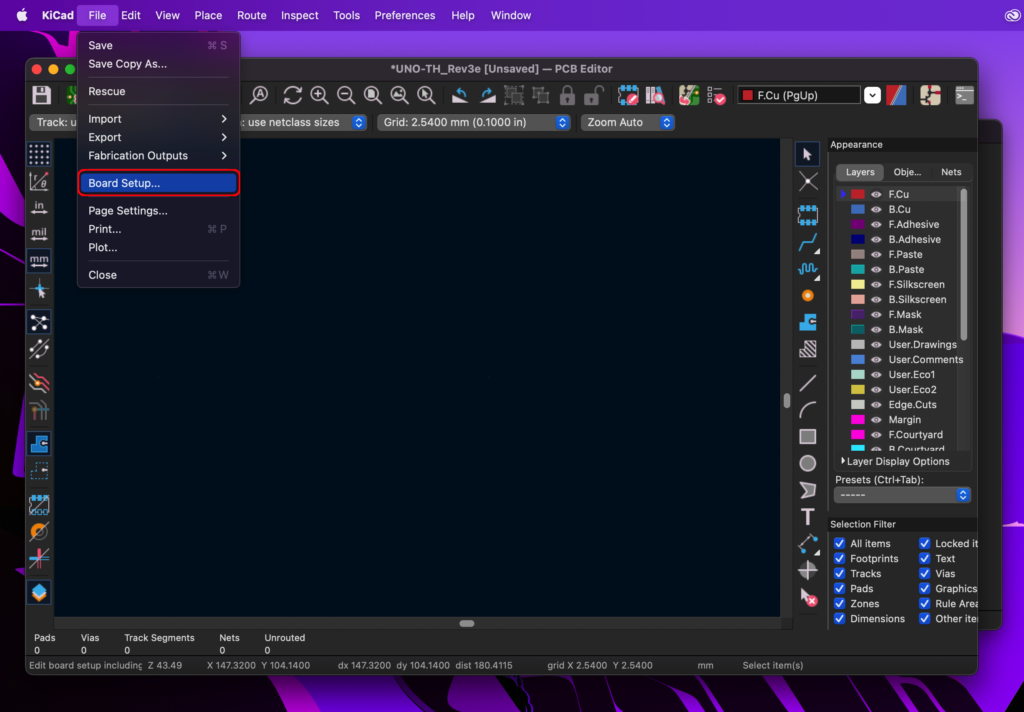
There are several different sections within the board setup menu accessible from the left-hand menu. Here you can select the appropriate section and enter the details from the fabricator.
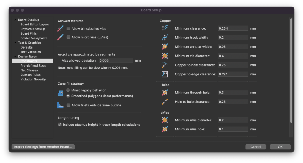
We can take a look again at the table from earlier and enter the parameters in KiCad. For reference the following table shows the menu location whereby each parameter should be entered.
| Parameter | PCBWay DFM Values | KiCad Menu |
| Number Of Layers | 1 – 10 | Board Stackup > Physical Stackup |
| Maximum PCB Dimension | 500 x 1100 mm | N/A (Defined by Edge.Cuts layer) |
| Board Size Tolerance | ±0.2mm | Design Rules > Constraints > Copper To Edge Clearance |
| Board Thickness | 0.2 – 2.4mm ±10% | Board Stackup > Physical Stackup > Thickness |
| Minimum Track | 0.1mm | Design Rules > Constraints > Minimum Track Width |
| Minimum Spacing | 0.1mm | Design Rules > Constraints > Minimum Clearance |
| Minimum Hole Size | 0.2mm ±0.08mm | Design Rules > Constraints > Minimum Via Diameter |
| Minimum Annular Ring | 0.15mm | Design Rules > Constraints > Minimum Annular Width |
| Minimum Legend Width | 0.15mm | Text & Graphics > Defaults > Line Thickness |
Conclusion
Design for manufacturing is an important part of printed circuit design and should almost certainly be considered for all boards being sent for external fabrication.
However it is not so difficult to incorporate DFM into a design with KiCad 6 once we know where to get the correct parameters from.
For further information regarding getting a board fabricated, I would highly recommend checking out this tutorial, which explains how to output manufacturing data.
Thanks so much for visiting my site! If this article helped you achieve your goal and you want to say thanks, you can now support my work by buying me a coffee. I promise I won't spend it on beer instead... 😏